A copper trace looks like a perfect wire on a schematic, yet every millimetre adds a few milliohms that become real voltage drop and heat at high current. This guide shows how to calculate that resistance by hand and with a calculator.
Trace resistance decides how much voltage you lose between a regulator and its load and how hot a power path runs. We cover the formula, copper thickness, temperature effects and two solved examples.

What Is PCB Trace Resistance?
PCB trace resistance is the DC resistance of a copper track on a printed circuit board, set by the resistivity of copper, the trace length and its cross section area. It is calculated with R = ρ × L ÷ (W × T), where W is the trace width and T is the copper thickness.
- R = ρ × L ÷ (W × T), with ρ of copper about 1.724 × 10 to the power minus 8 Ω·m at 20 °C
- 1 oz copper is about 35 µm thick, 2 oz about 70 µm
- 1 oz copper has a sheet resistance near 0.49 mΩ per square
- Resistance rises about 0.393 % for every °C above 20 °C
- A 100 mm × 0.5 mm, 1 oz trace is about 98.5 mΩ at 20 °C
PCB trace resistance follows the same physics as any conductor, explained in what is resistance. On a board the length is usually fixed by placement, so width and copper weight become the two levers you can actually change.
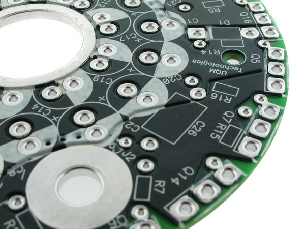
The board above mixes thin 2 oz control traces with very thick 20 oz copper for high current, a direct way to cut resistance. Epec classes 1/2 to 3 oz as standard copper and 4 to 20 oz as heavy copper.
PCB Trace Resistance Formula
The formula is the basic resistance law with the cross section written as width times thickness. Flux gives the resistivity of copper as about 1.724 × 10 to the power minus 6 Ω·cm at 20 °C, which equals 0.01724 Ω·mm² per metre.
R = ρ × L ÷ (W × T)
ρ = 0.01724 Ω·mm²/m at 20 °C
L, W, T in consistent units
In mm: ρ = 0.00001724 Ω·mm
Keep every dimension in the same unit, and the most common error is mixing millimetres for length with micrometres for thickness. With L, W and T all in millimetres, use ρ = 0.00001724 Ω·mm and the result comes out directly in ohms.
| Copper weight | Thickness (µm) | Thickness (mil) | Sheet resistance at 20 °C |
|---|---|---|---|
| 0.5 oz | 17.5 | 0.7 | 0.99 mΩ/sq |
| 1 oz | 35 | 1.4 | 0.49 mΩ/sq |
| 2 oz | 70 | 2.8 | 0.25 mΩ/sq |
| 3 oz | 105 | 4.2 | 0.16 mΩ/sq |
| 4 oz | 140 | 5.6 | 0.12 mΩ/sq |
The thickness values follow the Epec table of about 0.0014 inch per ounce, and the sheet resistance is simply ρ divided by thickness. Texas Instruments uses a practical 1 oz value of 34.8 µm in its application note on copper trace shunts.
Copper weight means ounces of copper spread over one square foot of board. One ounce over one square foot gives a layer close to 35 µm thick, which is why 1 oz and 35 µm are used as the same thing.
How to Calculate PCB Trace Resistance by Counting Squares
A quick way to estimate pcb trace resistance is to count squares, because a square of copper has the same resistance whatever its size. Divide the trace length by its width to get the number of squares, then multiply by the sheet resistance from the table.
Squares = L ÷ W
R = squares × sheet resistance
100 mm ÷ 0.5 mm = 200 squares
200 × 0.4926 mΩ = 98.5 mΩ at 20 °C
For a trace that changes width along its path, split it into straight sections, calculate each one and add them. Bends add roughly half a square at each corner, so do not ignore them on short, wide power traces.
Vias in the path add their own resistance, often more than a short trace segment, so read PCB via current capacity when a power path changes layers. Large copper pours behave like very wide traces, as covered in PCB copper pour guidelines.
Temperature Coefficient of Copper Resistance
Copper resistance rises with temperature at about 0.393 % per °C, which is a coefficient of 0.00393 per °C near room temperature. A trace that is 98.5 mΩ at 20 °C becomes about 129 mΩ at 100 °C, an increase of over 31 %.
R_T = R_20 × (1 + 0.00393 × (T minus 20))
At 100 °C: factor = 1 + 0.00393 × 80 = 1.314
98.5 mΩ × 1.314 = 129.4 mΩ
This rise in pcb trace resistance feeds back into heating, because more resistance means more I²R loss and a hotter trace. Texas Instruments reports that a copper trace shunt took more than 5 minutes to settle in some tests as it self heated, so always measure after the trace reaches a stable temperature.
Silver has slightly lower resistivity than copper, yet boards use copper because it is far cheaper and easy to plate. Aluminium has about 1.6 times the resistivity of copper, so an aluminium track would need a much larger cross section.
Voltage Drop and Power Loss in a Trace
Once you know the pcb trace resistance, the voltage drop is I × R and the power lost as heat is I² × R, the same Ohm law you use for any resistor. These numbers decide whether a 3.3 V rail still meets its tolerance at the far end of the board.
A drop of 100 mV is small on a 24 V rail but it is 3 % of a 3.3 V supply, which can push a processor below its limit. Low dropout regulators are especially sensitive, so check the margin against LDO dropout voltage when the regulator sits far from its load.
Thin traces with tiny currents, where resistance rarely matters.
Supply traces where drop and heat must be checked.
Shunt and Kelvin traces where milliohms matter.
Thick copper for tens of amperes.
Width for a safe temperature rise comes from IPC charts, and our PCB trace width calculator handles that part of the job. Resistance and width are linked, because a wider trace both runs cooler and drops less voltage.
PCB Trace Resistance Calculator
Enter length and width in millimetres, copper weight in ounces, operating temperature and load current. The defaults describe a 100 mm, 0.5 mm wide, 1 oz trace at 45 °C carrying 2 A.
T = 1 × 0.035 = 0.035 mm
R_20 = 0.00001724 × 100 ÷ (0.5 × 0.035)
R_20 = 98.51 mΩ
Factor = 1 + 0.00393 × 25 = 1.0983
R = 108.19 mΩ
Drop = 2 × 0.10819 = 216.4 mV
Loss = 2² × 0.10819 = 432.8 mW
A 216 mV drop would be a real problem on a 3.3 V rail, so this trace needs to be wider, shorter or on 2 oz copper. Doubling the copper weight alone halves the pcb trace resistance to about 54 mΩ and the loss to about 216 mW.
Second Solved Example: Motor Driver Trace
A motor driver carries 3 A through a 50 mm trace, 2 mm wide, on 2 oz copper that runs at 70 °C. The thickness is 0.070 mm, so R_20 = 0.00001724 × 50 ÷ (2 × 0.070) = 6.16 mΩ.
Factor at 70 °C = 1 + 0.00393 × 50 = 1.1965
R = 6.16 × 1.1965 = 7.37 mΩ
Drop = 3 × 0.00737 = 22.1 mV
Loss = 9 × 0.00737 = 66.3 mW
This trace is fine for power, but if the same copper is used as a current sense path the 7.37 mΩ would shift with every degree. That is why precise current sensing uses a real shunt resistor rather than raw copper unless the error budget allows it.
- No extra component cost
- No extra board space
- Handles high current easily
- Useful for rough overcurrent detection
- Resistance changes 0.393 % per °C
- Thickness varies from board to board
- Plating adds unknown copper on outer layers
- Needs calibration for good accuracy
Texas Instruments found that outer layer traces on its test boards plated to about 61 to 64 µm instead of the 34.8 µm assumed for 1 oz copper. After using the measured thickness, the average error of one tap point fell from about minus 45 % to about 4 %.
Field Tips and Design Checks
- Use the routed length, not the straight line distance
- Use finished width and real copper thickness
- Correct for operating temperature with 0.00393 per °C
- Add via and connector resistance to the path
- Check voltage drop against the rail tolerance
- Check I²R loss and temperature rise together
When you measure a low trace resistance, use a 4 wire milliohm meter with separate sense leads. A normal multimeter adds its own lead resistance, which can be larger than the trace you are trying to measure.
The return path carries the same current, so its resistance adds to the drop the load sees, which is explained in PCB return current path. A solid plane gives the lowest return resistance, as shown in ground plane PCB design.
Copper weight is chosen early in the PCB layer stackup, so do this resistance check before the stackup is frozen. For more layout rules on width, spacing and copper, see essential PCB design rules.
The video shows the counting squares idea on a real board with a milliohm meter, which is a good way to see sheet resistance in action. Try the same trace in our pcb trace resistance calculator and compare the numbers.
PCB Trace Resistance FAQ
Use R = ρ × L ÷ (W × T), with copper resistivity of about 0.01724 Ω·mm² per metre at room temperature. Keep length, width and thickness in the same unit so the result comes out in ohms.
Then correct for temperature by multiplying by 1 + 0.00393 × (T minus 20). This gives the real working resistance of the trace.
One ounce copper is about 35 µm thick, which gives a sheet resistance near 0.49 milliohms per square at room temperature. A square of any size has this same value, so only the ratio of length to width matters.
A trace 100 mm long and 0.5 mm wide is 200 squares. That gives roughly 98.5 milliohms at room temperature.
Yes, resistance is inversely proportional to width, so doubling the width halves the resistance for the same length and copper. Width is usually the easiest parameter to change in layout.
A wider trace also spreads heat over a larger area and runs cooler. This lowers the temperature correction and reduces resistance even further in real use.
Copper resistance rises by about 0.393 % for every degree Celsius above 20 °C, using a coefficient of 0.00393 per degree. At 100 °C a trace is roughly 31 % higher than at room temperature.
This matters for current sensing and power traces that run hot. Always calculate at the expected operating temperature, not at the room value.
The most common reason is thicker copper than assumed, because outer layers receive extra plating during fabrication. Texas Instruments measured about 61 to 64 µm on traces designed as 1 oz copper.
Measurement method also matters a lot at milliohm levels. Use a 4 wire meter so lead resistance does not hide the real value of the trace.
Make the trace wider, shorter or move it to thicker copper, and use several vias in parallel at layer changes. A copper pour or plane can replace a narrow trace for heavy currents.
Placing the regulator close to its load is often the cheapest fix of all. Remote sense lines can also correct the drop at the regulator output.
Related Articles
- PCB Trace Width Calculator
- PCB Via Current Capacity
- PCB Copper Pour Guidelines
- Thermal Vias for PCB Heat Dissipation
- PCB Design Fundamentals
External References
- Texas Instruments: Using a PCB Copper Trace as a Current Sense Shunt Resistor (PDF)
- Flux: How to Calculate PCB Trace Resistance
- Wikipedia: Electrical Resistivity and Conductivity
What We Learn Today
- PCB trace resistance follows R = ρL divided by width times thickness, with copper at 0.01724 Ω·mm² per metre at 20 °C.
- One ounce copper is about 35 µm thick with roughly 0.49 milliohm per square, so counting squares gives a fast estimate.
- Resistance rises about 0.393 % per degree, and the voltage drop and I squared R loss must be checked at the real operating temperature.