
Every signal that leaves a driver must come back to its source, and the route it takes home decides how much noise your board makes and receives. Get that route right and many crosstalk, ringing and EMI problems simply disappear.
Current always flows in a loop, and on a printed circuit board the second half of that loop is usually invisible on the schematic. Designing the return path deliberately is one of the cheapest ways to pass EMC tests and keep signals clean.

What Is a Return Path in a PCB?
A return path is the route that current takes from the load back to the source after travelling out along a signal trace. Since every circuit is a closed loop, as Kirchhoff current law tells us, the return current is exactly equal to the signal current, only flowing the other way.
On a schematic the return is just a ground symbol, so it feels free and automatic. On a real board that current flows through copper planes, vias and capacitors, and its exact route controls inductance, noise and radiation, as explained in what is signal integrity.
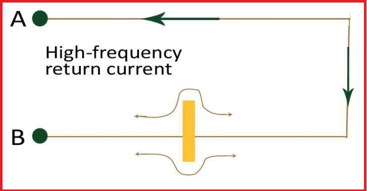
The image shows what happens when a slot cuts the return path under a trace. The current cannot flow straight under the signal, so it spreads around the slot, creating a large loop that behaves like an antenna.
Where Does Return Current Really Flow?
At low frequency, current chooses the path of least resistance, which is usually the shortest straight line through the plane. At high frequency, it chooses the path of least inductance, and that path lies directly beneath the signal trace because it gives the smallest loop area.
Sierra Circuits explains that between about 1 and 100 kHz the return flows mainly through the path of least resistance. Around 500 to 1000 kHz the current splits between the two routes, and from about 10 to 100 MHz the majority flows underneath the trace.
This switch over is why a board with a poor return path can work at audio frequencies yet fail with fast digital edges. The important point is that rise time, not clock frequency, decides the spectrum, so a 1 MHz clock with 1 ns edges is still a high frequency signal.
A fast edge contains energy up to a knee frequency of about 0.35 divided by the rise time. A 1 ns edge therefore has strong content near 350 MHz, even if the clock itself runs at only a few megahertz.
Why the Return Path Decides Noise and EMI
The signal and its return form a current loop, and loop area sets both the inductance and the strength of the radiated field. A tight loop radiates little and picks up little, while a large loop acts as an efficient antenna, which is the root cause behind many cases of electromagnetic interference.
When the return path is broken, the trace also sees an impedance change, which causes reflections and ringing. The loss of a solid reference undoes careful work on controlled impedance traces, because the trace impedance assumes a continuous plane beneath it.
Wide return loops also overlap the loops of neighbouring traces, so magnetic coupling rises. This is a major source of the coupling discussed in PCB crosstalk reduction, and of shared inductance that produces ground bounce when many outputs switch together.
7 Essential Return Path Rules
Rule one depends on a good stackup, where each signal layer sits next to a solid plane. The article on PCB layer stackup design shows how a four or six layer build gives every trace an adjacent reference.
Before routing, turn on the plane layers and look for slots formed by rows of clearance holes under connectors and BGAs. Rows of antipads can merge into a long gap that silently cuts the return under many traces.
Plane Splits and Slots
Texas Instruments warns in its High Speed Layout Guidelines that split ground planes act as slot antennas and radiate. It also states that a trace routed over a gap creates a large loop area, because the return current cannot flow beside the signal.
TI recommends a continuous ground plane wherever possible. If a split is truly required, for example between isolated sections, route no fast traces across it and provide a defined bridge or stitching capacitor where crossing is unavoidable.
Two separate planes with a gap between them.
A narrow opening in one plane, often from routing on a plane layer.
Clearance holes that merge into a gap.
Mixed signal boards usually keep one solid ground and partition parts instead of cutting the return path. This approach is covered in ground plane PCB design, where analog and digital sections sit on separate regions of the same plane.
Return Path at Layer Changes
When a signal moves through a via from one layer to another, its reference plane usually changes too. If both layers reference ground, a ground via placed next to the signal via gives the return path a short way to jump between planes, following the via ideas in PCB via types.
TI suggests placing ground vias around the signal via so the structure behaves like a small coaxial line. Without them, the return current spreads out to find the nearest connection between planes, increasing the loop and coupling noise into the cavity between planes.
If the signal changes from a ground reference to a power plane reference, the return must cross between two different nets. A stitching capacitor placed close to the via gives that high frequency path, and the same capacitors help as described in how decoupling capacitors work.
The return current in a plane is not a thin line but spreads out under the trace, most of it within a few trace heights of the centre line. That is why a thinner dielectric between trace and plane gives a tighter, quieter loop.
Stitching Via Spacing Formula
A common rule of thumb places ground stitching vias no farther apart than one twentieth of the wavelength at the highest frequency of concern. The wavelength inside the board is shorter than in air, because signals travel slower in the dielectric.
Maximum via spacing = λ ÷ 20
Example: f = 1000 MHz, FR4 εr = 4.2
λ = 300 mm ÷ (1 × √4.2) = 300 ÷ 2.049 = 146.4 mm
Spacing = 146.4 ÷ 20 = 7.32 mm
Via Spacing Calculator
Second worked example: for a 1 ns edge, the knee frequency is 0.35 ÷ 1 ns = 350 MHz. With εr = 4.2, the wavelength is 300000 ÷ (350 × 2.049) = 418.3 mm, so the spacing limit is about 20.9 mm.
Many designers simply keep vias within a few millimetres along fast edges. Tighter spacing costs little and keeps the return path short for harmonics too.
Loop Area and Decoupling Capacitors
Power pins also need a clean return path, because each switching event draws a burst of current from the nearest capacitor. The inductance of that loop sets how well the capacitor can supply the burst.
TI advises placing the lowest value capacitor as close as possible to the device and connecting its pad directly with a via to the ground plane. Short, wide connections and vias placed side by side keep this loop small and the supply quiet.
Put the decoupling capacitor via right at the pad, not at the end of a thin trace. A few millimetres of extra trace can add several nanohenries and cancel much of the benefit of a good capacitor.
Return Path Design Checklist
- Every fast signal layer has an adjacent solid reference plane.
- No high speed trace crosses a split, slot or antipad chain.
- Ground vias sit beside every signal via that changes layers.
- Stitching capacitors bridge any change between power and ground references.
- Decoupling capacitors connect through short via pairs.
- Fast traces stay several trace widths away from plane edges.
- Ground pours are stitched to the plane at regular spacing.
- Connectors carry enough ground pins next to fast signals.
Troubleshooting a Broken Return Path
Symptoms of a poor return path include failing radiated emissions near a particular clock harmonic, intermittent data errors on a bus and noise appearing on sensitive analog channels. Review the plane layers under the failing net first, before adding filters such as those in ferrite bead vs common mode choke.
On cables, the same principle explains why every signal wire needs a nearby return conductor, as in twisted pairs and shields. Off board loops caused by multiple ground connections are covered in ground loop causes and prevention, and the EMC side in EMI vs EMC.
- Smaller loop area and lower radiated emissions.
- Stable trace impedance and fewer reflections.
- Less crosstalk between neighbouring nets.
- Quieter supplies and less ground bounce.
- Higher chance of passing EMC tests first time.
- Extra layers raise board cost.
- Ground vias consume routing space.
- Stitching capacitors add parts and assembly cost.
- Solid planes limit routing on inner layers.
- Isolation requirements may force real splits.
Applications That Need Careful Returns
Industrial products sold in India and abroad typically face IEC 61000 immunity and CISPR emission tests. A sound return path design is part of the essential PCB design rules that make these tests far easier, alongside the broader advice in signal integrity in high speed PCB design.
TI High Speed Layout Guidelines
Grounding and Noise Video by Rick Hartley
Return Path FAQ
It is the route the current takes from the load back to its source after travelling along a signal trace. The return carries exactly the same current as the signal, only in the opposite direction.
On most boards this current flows through a ground or power plane. Its route decides loop area, inductance and how much noise the circuit radiates.
At high frequency, current follows the path of lowest inductance rather than lowest resistance. The lowest inductance route is directly beneath the signal, since that gives the smallest loop.
Sierra Circuits notes that most return current flows under the trace from about 10 to 100 MHz. At low frequencies it takes the shortest resistive path instead.
A split forces the return current to detour around the gap. That detour makes a large loop that radiates strongly and picks up noise from nearby circuits very easily.
Texas Instruments warns that split planes act as slot antennas. Its guidance is to keep a continuous ground plane under every fast return path wherever the design allows it.
It is a via that connects ground areas on different layers to each other. Placed next to a signal via, it lets the return current jump between planes close to the signal.
Rows of stitching vias also tie ground pours to the main plane. This stops floating copper from resonating and radiating at high frequencies.
You need one when a signal changes from a ground reference to a power plane reference. The return current must then cross between two different nets.
A small ceramic capacitor placed close to the via gives that high frequency route. Without it, the return current wanders to the nearest decoupling capacitor and enlarges the loop.
A common rule keeps them within one twentieth of the wavelength at the highest frequency of concern. On FR4 at 1 GHz that works out to roughly 7 millimetres.
Use the knee frequency of your fastest edge rather than the clock rate. Closer spacing adds margin for harmonics and usually costs very little on most boards.
The edge rate matters more than the clock frequency. A slow clock with nanosecond edges still contains high frequency energy that needs a tight return path.
Truly slow signals such as relay drives or analog sensor lines are more forgiving. Even so, sensitive analog lines still benefit from a solid ground reference and a short return path beneath them.
Related Articles
- Ground Plane in PCB Design
- PCB Layer Stackup Design
- PCB Crosstalk Reduction
- Controlled Impedance PCB Traces
- Ground Bounce in PCB Simultaneous Switching
External References
- High Speed Layout Guidelines SCAA082A, Texas Instruments
- How to Handle Current Return Path for Better Signal Integrity, Sierra Circuits
- Ground Plane, Wikipedia
What We Learn Today
- At high frequency the return path lies directly under the signal trace, because current follows the route of least inductance and smallest loop area.
- Plane splits, slots and merged antipads force the return current to detour, turning the loop into a slot antenna that radiates and couples noise.
- Ground vias beside signal vias, stitching capacitors at reference changes and via fences spaced near one twentieth of a wavelength keep loops tight.