A plated via is only a thin copper tube, so a power path that jumps between layers can choke at the via long before the trace complains. Sizing the barrel, the plating and the number of vias correctly keeps the joint cool and the voltage drop tiny.
Every high current net that changes layers passes through one or more plated vias. This guide shows how to estimate via current capacity from hole size, plating and allowed temperature rise, and how many vias a real power path needs.
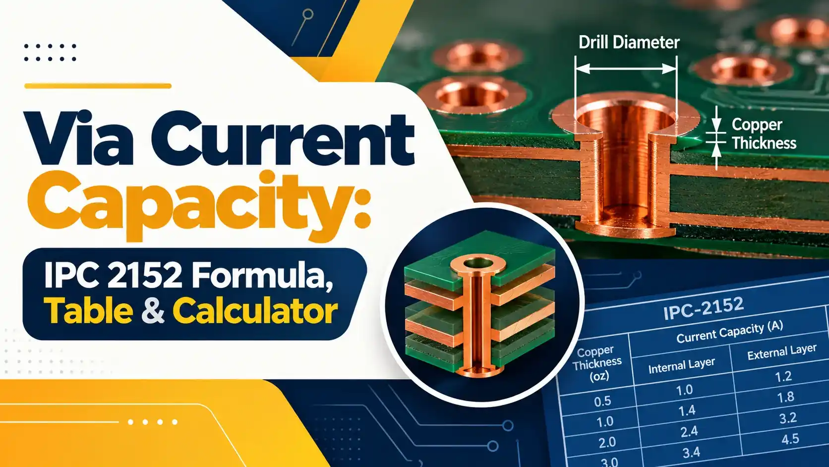
What Is Via Current Capacity?
Via current capacity is the steady current a plated through via can carry while its copper barrel stays within an allowed temperature rise above the board, usually 10 °C to 30 °C. It depends mainly on the barrel cross section, which comes from the finished hole diameter and the plated via wall thickness.
- A standard 0.3 mm via with 25 µm plating carries about 1.9 A for a 10 °C rise using the outer layer IPC curve fit.
- Barrel area = π × t × (d + t), where d is the finished hole and t is the plating thickness.
- IPC 6012 asks for an average hole wall copper of 20 µm for Class 2 and 25 µm for Class 3.
- For more current, place vias in parallel and divide the total current by the current per via.
- Size the connected traces first, because they set most of the via temperature.
In practice via current capacity answers a simple question: will this via get hot, and how many do I need? The answer links directly to PCB trace width, since a via and the trace feeding it should carry the same current with similar heating.
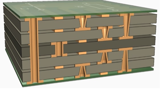
A via in a 1.6 mm board is a copper tube roughly as long as the board is thick, with a wall thinner than a human hair. Its copper area can still match a narrow power trace, which is why one via is often enough for signal nets.
Via Barrel Cross Section and Plating Thickness
The copper that carries current in a through via is the plated ring on the hole wall. If d is the finished hole diameter and t is the wall thickness, the ring area is π × t × (d + t), which is the difference between two circles.
Plating thickness therefore affects via current capacity as much as hole size. JLCPCB summarises IPC 6012 as asking for an average hole wall copper of 20 µm (0.8 mil) for Class 2 boards and 25 µm (1.0 mil) for Class 3 boards, with thin points allowed down to 18 µm and 20 µm.
Ask your fabricator which class they actually build to, because the two classes differ by 5 µm on the hole wall. A thicker wall also helps the via survive thermal cycling, which links to the reliability topics in essential PCB design rules.
Via Current Capacity Formula
The closed form used by most quick calculators is the IPC 2221 conductor equation, I = k × ΔT^0.44 × A^0.725, with A in square mils and ΔT in °C. Sierra Circuits lists k as 0.048 for external conductors and 0.024 for internal conductors.
For a via, the barrel area replaces the trace cross section in that equation. This article uses the outer layer constant 0.048 as a common simplification, and the internal constant 0.024 gives a conservative lower bound.
I = 0.048 × ΔT^0.44 × A^0.725
R = ρ × L ÷ A
Solved example:
d = 0.3 mm, t = 25 µm, ΔT = 10 °C, L = 1.6 mm
A = π × 0.025 × 0.325 = 0.02553 mm²
A = 0.02553 ÷ 0.00064516 = 39.56 mil²
I = 0.048 × 2.754 × 14.39 = 1.90 A
R = 0.0168 µΩ m × 1.6 mm ÷ A = 1.05 mΩ
5 A ÷ 1.90 A = 2.63, so use 3 vias
The resistivity of copper, 1.68 × 10 to the power minus 8 Ω m at 20 °C, is taken from the Sierra Circuits table. With 1.05 mΩ per via, even 1.9 A drops only about 2 mV, so heat rather than voltage drop sets the limit, as Ohm’s law shows.
Via Current Calculator
For a conservative via current capacity, halve the calculator result for vias buried deep in a thick multilayer board. If the design still works at half the current, you have a comfortable margin.
Via Current Capacity Table for Common Hole Sizes
The via current capacity table below applies the same formula to popular finished hole sizes, for both Class 2 and Class 3 plating. Values are per via, outer layer constant, and rounded to two decimals.
| Finished Hole | Plating | Area, mil² | 10 °C Rise | 20 °C Rise | 30 °C Rise |
|---|---|---|---|---|---|
| 0.2 mm | 20 µm | 21.43 | 1.22 A | 1.65 A | 1.98 A |
| 0.2 mm | 25 µm | 27.39 | 1.46 A | 1.98 A | 2.36 A |
| 0.25 mm | 25 µm | 33.48 | 1.69 A | 2.29 A | 2.73 A |
| 0.3 mm | 20 µm | 31.16 | 1.60 A | 2.17 A | 2.59 A |
| 0.3 mm | 25 µm | 39.56 | 1.90 A | 2.58 A | 3.08 A |
| 0.4 mm | 25 µm | 51.74 | 2.31 A | 3.13 A | 3.75 A |
| 0.5 mm | 25 µm | 63.91 | 2.69 A | 3.65 A | 4.37 A |
| 1.0 mm | 25 µm | 124.78 | 4.37 A | 5.93 A | 7.09 A |
Going from Class 2 to Class 3 plating on a 0.3 mm via raises the estimate from 1.60 A to 1.90 A at a 10 °C rise. That is close to a 19 percent gain without changing the drill size at all.
How Many Vias for High Current?
For a power net, divide the total current by the current per via and round up. A 10 A motor driver or buck converter output with 0.3 mm vias at a 10 °C rise needs 10 ÷ 1.90 = 5.3, so six vias, and many designers add one or two more as margin.
Vias packed tightly together heat each other, so the simple division is slightly optimistic. Spread them along the width of the trace or pour, roughly one via pitch apart, so that current enters every barrel evenly.
For layer changes into a solid ground plane, the plane spreads heat very well, so vias landing in planes run cooler than vias joining two thin traces.
Why Vias Often Run Cooler Than Traces
Douglas Brooks and Johannes Adam tested this in Signal Integrity Journal and found that a via carrying the same current as its traces usually runs at a temperature close to the trace. In their measurements a 27 mil trace at 6.65 A reached about 114 °C while the via reached about 109 °C.
With a 200 mil trace at 8.55 A the trace measured about 40.5 °C and the via about 44.5 °C, only a few degrees higher. Their conclusion is that the connected traces, not the via current alone, mainly set the via temperature.
The reason is that FR4 conducts heat better than still air, so the via sheds heat into the laminate and planes. The same physics lets thermal vias pull heat out of hot packages, a topic covered in its own guide.
IPC 2152 Approach for Vias
IPC 2152, published in August 2009 under the title Standard for Determining Current Carrying Capacity in Printed Board Design, replaced the old IPC 2221 charts for conductor sizing. Its table of contents includes sections on vias, conductor to via to plane paths and microvias.
Sierra Circuits explains that under IPC 2152 the via cross section should match the cross section of the trace it connects. In other words, size the trace first, then make sure the total barrel area of all vias in that path is at least equal to the trace copper area.
For example, a 1 oz outer trace (35 µm, about 1.38 mil thick) that is 29 mil wide has about 40 mil² of copper, almost exactly one 0.3 mm via with 25 µm plating. Checking the stack in PCB layer stackup design tells you which copper weights apply to each layer.
Write the plating class and minimum hole wall copper in your fabrication drawing notes. Without that line, you are designing to 25 µm while the fabricator may legally deliver 20 µm.
Via Current Capacity Mistakes and Troubleshooting
| Symptom | Likely Cause | Fix |
|---|---|---|
| Hot spot at a layer change | Too few vias for the current | Add vias using the calculator count |
| Voltage drop at the load | Thin plating or long thin traces | Specify Class 3 plating, widen traces |
| Via cracks after thermal cycling | Thin barrel, high aspect ratio | Larger drill, thicker plating, lower rise |
| Only one via of a group runs hot | Vias bunched at one end of the pour | Spread vias across the current path |
High current paths also affect noise, because every via adds a little inductance to the loop. Placing several vias near decoupling capacitors lowers that inductance and helps power integrity, alongside ground bounce control.
- Total current and allowed temperature rise are written down for each power net.
- Plating class and minimum hole wall copper are stated in the fab notes.
- Via current capacity per layer change covers the load plus margin.
- Vias are spread across the full width of the trace or pour.
- High current vias connect to planes without thin thermal relief spokes.
- Prototype temperature is checked at full load with a thermal camera.
- Cooler joints and longer board life.
- Very low voltage drop across layer changes.
- Lower loop inductance with parallel vias.
- Uses a trace curve fit, not via specific test data.
- Ignores heat sinking from planes and nearby copper.
- Ignores mutual heating of tightly packed vias.
Where Via Current Capacity Matters Most
In industrial boards, the 24 V field supply often feeds dozens of channels, so a single via in that rail can quietly become the weakest link. Good habits from PCB design fundamentals and signal integrity practice apply to power paths too.
IPC 2152 Table of Contents PDF
Video on PCB Via Current
Via Current Capacity FAQ
A standard 0.3 mm via with 25 µm plating carries about 1.9 A for a 10 °C rise using the outer layer formula. The same via with 20 µm plating carries about 1.6 amps.
Larger holes and thicker plating raise the figure, but not in direct proportion. Always check the result against the temperature rise you can accept on your board.
Divide the total current by the current per via and round up to the next whole number. With 0.3 mm vias at about 1.9 A each, that gives six vias for 10 amps.
Add one or two more for margin, since tightly packed vias heat each other. Spread them across the trace width so every via shares the load evenly.
Yes, because a larger hole gives a longer copper ring and therefore more conducting area. Plating thickness matters just as much, since it sets how thick that ring is.
Current grows with area to the power 0.725, so doubling the area raises current by about 65 percent. Several small vias are usually better than one very large via.
IPC 2152 treats the via barrel as a conductor and suggests that its cross section should match the trace it connects. If the trace is safe, a via of equal copper area runs at a similar temperature.
In practice, add up the barrel area of all vias in a path. Make sure that total is at least as large as the trace copper area feeding them.
Epoxy or resin filled vias carry the same current as open vias, because the fill adds no copper. They mainly help with flat pads, solder wicking and via in pad designs.
Copper filled or extra plated vias do raise the conducting area and lower resistance. They cost more, so many designers simply add more standard vias instead.
Not usually, according to tests by Douglas Brooks and Johannes Adam. Vias with the same copper area as their traces ran close to the trace temperature, sometimes a few degrees cooler.
The board laminate carries heat away from the barrel better than still air cools an outer trace. Planes connected to the via make it run cooler still.
The formula sets current by how much heating you allow above the surrounding board. A 30 °C rise allows more current than a 10 °C rise for the same via.
Pick the rise from your hottest ambient and the laminate rating. Most designers use 10 to 20 degrees for long life and reliable solder joints.
Related Articles
- Thermal Vias for PCB Heat Dissipation
- PCB Via Types: Through Hole, Blind and Buried
- PCB Trace Width Calculator
- PCB Layer Stackup Design
- Ground Plane PCB Design
External References
- IPC 2152 Standard for Determining Current Carrying Capacity in Printed Board Design, Table of Contents
- How to Design a Via With Current Carrying Capacity, Sierra Circuits
- Via (electronics), Wikipedia
What We Learn Today
- Via current capacity comes from the plated barrel area, π × t × (d + t), so plating thickness matters as much as the drill size you choose.
- A 0.3 mm via with 25 µm plating carries about 1.9 A for a 10 °C rise, and parallel vias share larger currents when spread evenly.
- Under IPC 2152, match the total via barrel area to the trace copper area, because the traces largely set the via temperature.