
Most people leave their PCB software on its default trace width and never think about it again. That's fine for a signal wire, but it's exactly how power traces end up scorched, discolored, or quietly failing months after the board ships.
A PCB trace width calculator tells you how wide a copper trace needs to be to carry a given current without overheating, based on the IPC-2221 standard.
Let's start with the honest version of how most people actually design their first few circuit boards: you drop a copper path, the software defaults to something like 10 mils, and you move on. For low-current signal lines, that's genuinely fine. Nobody needs to lose sleep over the trace feeding a status LED.

Power traces are a different story entirely. Feed a few amps through an undersized trace and you're not just risking a warm board, you're risking a trace that discolors, delaminates from the substrate, or in the worst case acts exactly like a fuse and burns open. This is where the math actually matters, and thankfully it isn't complicated once you've seen it once.
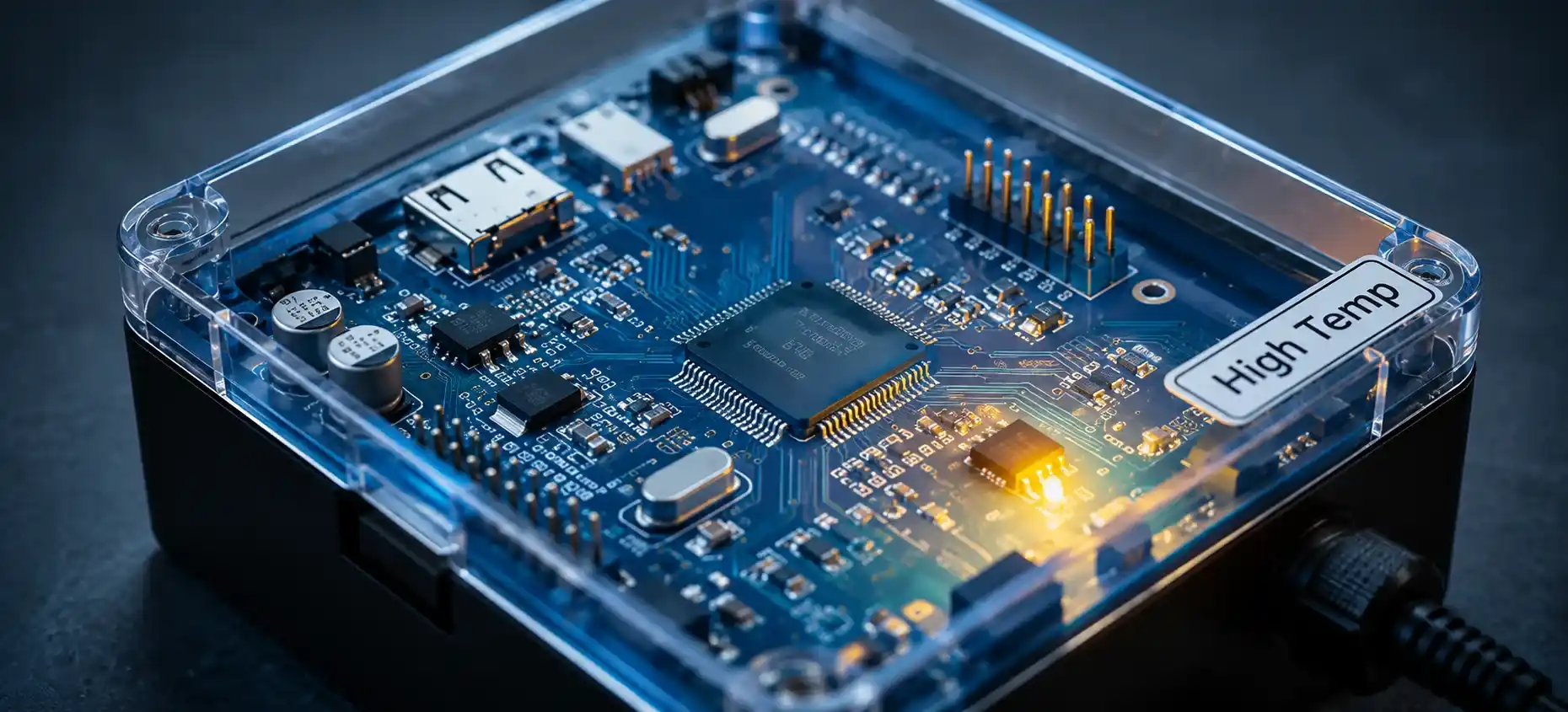
Why PCB Trace Width Comes Down to Heat, Not Just Current
Every trace has resistance, and current flowing through resistance always makes heat. That's just Joule heating, the same reason a resistor gets warm under load. A copper trace is really just a very low-value, very flat resistor, and it heats up exactly the same way.
The question a trace width calculation actually answers isn't "will this trace carry the current." Copper carries current just fine at almost any width, right up until it melts. The real question is: how much will this specific trace heat up above the surrounding air while carrying that current, and is that temperature rise something you're comfortable with?
That's the entire idea behind the IPC-2221 standard, which is still the most widely used reference for this calculation even though it dates back to empirical heating tests from decades ago. It ties current, trace geometry, and an allowable temperature rise together into one formula.
The IPC-2221 Formula for Copper Sizing, Explained Plainly
Here's the actual formula, and then we'll walk through exactly what each piece means.
Current formula: I = k × ΔT0.44 × A0.725
Rearranged to solve for area:
A = (I / (k × ΔT0.44))1/0.725
I = current in amps, ΔT = allowed temperature rise in °C
A = cross-sectional area in mil², k = 0.048 external, 0.024 internal
Once you have the required area, getting to a physical trace width just means dividing by how thick your copper is. That thickness comes from the copper weight, and this is where a lot of people get genuinely confused the first time.
Copper weight is specified in ounces per square foot, which sounds like a strange way to measure thickness until you realize it's really describing how much copper mass is spread over a given area. One ounce of copper spread over a square foot works out to a thickness of 1.378 mils, about 35 microns.
Two ounce copper is simply double that, 2.756 mils. Once you have the area from the formula above, dividing by the thickness in mils gives you the trace width in mils.
Why External and Internal Trace Width Requirements Aren't the Same
Look closely at that k value in the formula and you'll notice it's exactly half for internal layers compared to external ones, 0.024 versus 0.048. That's not an arbitrary safety margin, it reflects something genuinely physical about how heat actually leaves a trace.
External Layer Traces
Sitting on the top or bottom of the board, these traces are exposed directly to air. Air convection carries heat away efficiently, which is exactly why external traces get the more generous k value of 0.048.
Internal Layer Traces
Buried between layers of FR4 laminate, these traces have no air contact at all. FR4 is a fairly poor thermal conductor, so heat has a much harder time escaping, hence the lower k value of 0.024.
Because of the math's 0.725 exponent, halving k doesn't just double the required area, it actually works out closer to 2.6 times the area for the same current and temperature rise. In practical terms, an internal trace carrying the same current as an external one typically needs to be roughly twice as wide to stay at the same temperature. That's a big enough difference that it should genuinely influence your stackup decisions, not just your copper sizing.
Try It: PCB Trace Width Calculator
Enter your current, allowed temperature rise, copper weight, and layer type to get the minimum trace width the IPC-2221 formula recommends.
A Few Worked Examples to Build Intuition
Numbers stick better with real examples attached to them, so here are a few common situations run through the same calculator above, all at a conservative 10°C rise on 1 oz copper.
| Scenario | Current | Layer | Approx. Width Needed |
|---|---|---|---|
| USB 2.0 power line | 0.5A | External | ~5 mils (round up to 10 mil minimum) |
| Typical power rail | 2A | External | ~31 mils |
| Same rail, buried layer | 2A | Internal | ~65 mils |
| Small motor driver | 4A | External | ~75 mils |
| High-current motor driver | 10A | External | ~300 mils |
Notice that last row. Three hundred mils is 7.6mm, which on a lot of boards is simply not available as a single straight trace. This is exactly the point where real designs start reaching for other tools: heavier copper, like 2oz or even 4oz, splitting the current across two or three parallel traces on different layers, or in genuinely high-current cases, soldering an actual copper bus bar onto the board instead of routing it as a trace at all.
Voltage Drop Is the Part People Forget
Everything above answers one question, will the trace overheat. It says nothing about whether the voltage arriving at the far end of that trace is still the voltage you designed for.
A trace, no matter how well it handles heat, still has real resistance, and that resistance times current is a real voltage drop. On a long copper run carrying meaningful current, that drop can genuinely matter, especially if you're feeding a sensitive analog circuit or a microcontroller that's picky about its supply voltage.
The fix, when it matters, is usually simple: keep high-current traces as short as the layout allows, and don't be shy about going wider than the thermal minimum if the extra copper also buys you a smaller voltage drop. Wider and shorter is almost always better for both heat and voltage at the same time.
Here's a quick way to picture it. A 50mm run of 1oz copper at 30 mils wide carries roughly 0.02 ohms of resistance. Push 2A through that and you lose about 40mV, which is nothing for a power rail but could genuinely matter if that same copper is feeding a precision sensor reference where every millivolt counts.
The rule of thumb worth remembering is this: thermal sizing and voltage drop sizing are two separate calculations that happen to use the same copper. Do the heat math first, then check the drop on anything long or voltage-sensitive, and widen the copper again if the numbers don't sit well with you.
Common Copper Sizing Mistakes Worth Avoiding
Leaving Every Trace at the Software Default
A flat 10 mil default across an entire board might be fine for signal lines, but it will let a power trace run hot without any warning from your layout tool.
Forgetting Internal Traces Need Extra Width
Copying an external trace's width straight onto an internal layer, without accounting for that roughly 2.6x area difference, is one of the most common oversights in multilayer designs.
Treating the Calculator's Number as Final
The IPC-2221 output is a minimum, not a target. Rounding up for manufacturing tolerance and long-term reliability margin costs you almost nothing in board space on most designs.
Where Trace Width Calculations Matter Most
Power Supply Boards
Input and output rails often carry the highest sustained currents on the entire board.
Motor Drivers
Motor phase currents can spike well above a design's average current draw.
LED Strip Controllers
Long LED runs add up in current even though each individual LED draws very little.
Watch: How to Calculate PCB Trace Width
This video from Digi-Key walks through sizing a power trace using the same IPC-2221 approach covered above.
FAQs on PCB Trace Width Calculations
External References
What we learn today
- Trace width calculations answer a heat question, not just a current question: how much will this trace warm up above ambient while carrying its load.
- The IPC-2221 formula, I = k × ΔT^0.44 × A^0.725, ties current, temperature rise, and cross-sectional area together, with k set by whether the trace is external or internal.
- Internal traces need roughly 2.6 times the area of an external trace to hit the same temperature rise at the same current, since they can't shed heat into open air.
- Copper weight in ounces sets trace thickness directly, so heavier copper always means a narrower trace can carry the same current.
- Trace width only solves the heat problem. Voltage drop on long, high-current traces is a separate consideration worth checking on its own.