
FR4 is a poor heat conductor, but a grid of small plated holes under a hot chip can drop its temperature by tens of degrees.
Power ICs, regulators and MOSFETs push heat into the board through their exposed pads. Plated holes carry that heat down to inner planes and the bottom copper, where it can spread and escape.

What Are Thermal Vias?
Thermal vias are plated through holes placed under or near a hot component to conduct heat from the top copper to inner planes and the bottom layer. They work because plated copper conducts heat about a thousand times better than FR4, a point covered in thermal conductivity.
Sierra Circuits gives copper a thermal conductivity of about 385 W per m K. FR4 is only about 0.3 W per m K, so heat struggles to pass through the laminate alone.
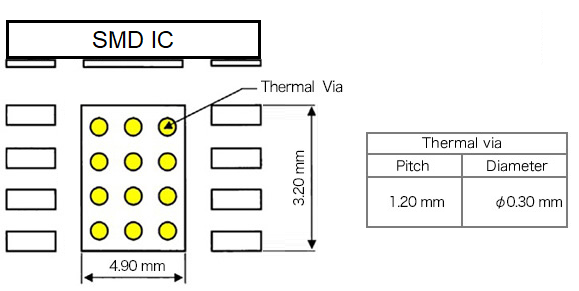
They are the same plated holes described in PCB via types, placed for heat rather than signals. Most are simple through hole vias.
An exposed pad package such as QFN or DPAK relies on these vias for most of its cooling. Datasheets often show a recommended via pattern.
How Heat Flows Through the Board
Thermal vias alone do not remove heat, they move it to a larger copper area. Without enough copper on the other side, the benefit is small.
Solid inner planes from the layer stackup spread heat well. A ground plane often doubles as the heat spreader.
6 Practical Thermal Vias Rules
Sierra Circuits recommends the 1 mm to 1.2 mm spacing to prevent solder wicking. ROHM warns that vias of 0.3 mm or larger inside an exposed pad can draw solder away during reflow.
ROHM also shows that more vias lower thermal resistance, but even one via directly under the source makes a large difference. Returns diminish after a dense grid is reached.
Via Thermal Resistance Formula
A = π × (r outer² minus r inner²)
R total = R via ÷ N
Worked example, 1.6 mm board, 0.3 mm drill, 25 µm plating:
A = π × (0.150² minus 0.125²) mm² = 0.0216 mm²
R via = 0.0016 m ÷ (385 × 0.0000000216 m²) ≈ 192 °C per W
16 vias in parallel ≈ 12 °C per W
Filling thermal vias with copper or conductive epoxy lowers resistance further. Plain resin filled vias mainly help with soldering, not heat.
This formula ignores spreading resistance in the copper planes, so treat it as the best case. Thermal simulation or a quick measurement with a thermocouple on the prototype gives the full picture.
Via Finish Options
Unfilled plated holes.
Covered by solder mask.
Filled with resin then capped.
Solid copper barrel.
Via in pad with fill and cap, often called VIPPO, gives a flat surface under fine pitch parts. It costs more, so use it only where needed.
Discuss options with your fabricator early, alongside the rules in essential PCB design rules.
Where Thermal Vias Matter
A linear regulator can dissipate several watts, so via arrays are essential. Board level airflow is covered in electronic cooling fans.
Via Array Calculator
Doubling the via count halves the array resistance in this simple model. Real gains are smaller because spreading resistance remains.
- Low cost heat path.
- Works with standard fabrication.
- Uses existing planes as heat spreaders.
- Reduces component temperature.
- Solder wicking in pads.
- Less routing space on inner layers.
- Filled vias add cost.
- Little effect without copper area.
ROHM Thermal Design Guide PDF
Thermal PCB Design Tips Video
Thermal Vias FAQ
Related Articles
- PCB Via Types
- PCB Layer Stackup Design
- PCB Trace Width Calculator
- PCB Design Fundamentals
- What Is Thermal Conductivity
External References
- PCB Layout Thermal Design Guide, ROHM
- How Thermal Vias Dissipate Heat, Sierra Circuits
- Thermal Via, Wikipedia
What We Learn Today
- Plated copper barrels move heat far better than FR4.
- Size, pitch and placement under the hot spot decide performance.
- Connect thermal vias to large copper planes and manage solder in pads.