
A low dropout linear regulator turns a slightly higher, noisy supply into a quiet and steady rail with only a few parts. Knowing its dropout, rejection, noise, stability and heat limits is what separates a clean design from a hot, oscillating one.
Microcontrollers, ADCs and sensors all need a clean supply rail close to the input voltage. An LDO regulator delivers that rail with very little headroom, provided you respect its dropout, stability and thermal limits.
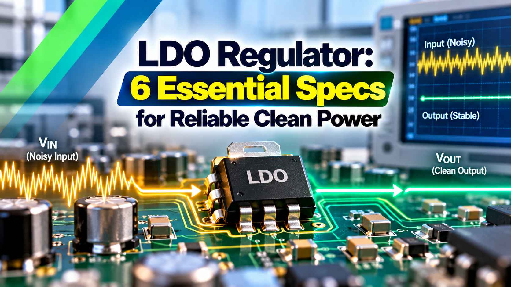
What Is an LDO Regulator?
An LDO regulator, or low dropout regulator, is a linear voltage regulator that keeps its output steady even when the input is only slightly above the output, often by 100 to 300 mV. It belongs to the linear family compared in linear vs switching voltage regulators, and it trades efficiency for simplicity and low noise.
Inside, an error amplifier compares a fraction of the output with a reference voltage and drives a pass transistor like a variable resistor. Whatever voltage is not needed at the output is dropped across that transistor and turned into heat.

The diagram shows the four blocks every design shares: the pass element, the error amplifier, the reference and the feedback divider. The reference is usually a bandgap circuit, which is far more stable than a simple Zener diode reference.
LDO Regulator Dropout and the Pass Element
Dropout voltage is the smallest difference between input and output at which the regulator still holds its output within specification. Below this headroom the pass transistor is fully on and the output simply follows the input minus a small drop.
Analog Devices notes that standard regulators with NPN pass transistors typically need about 2 V of dropout, because the base drive can only be pulled up to the supply rail. That is why a classic 7805 cannot make 5 V from a 5.5 V source.
Classic 78xx style regulator; dropout near 2 V.
Early low dropout type; dropout of a few hundred mV but high base current.
Dropout equals RDS on times load current, with tiny ground current.
Needs a gate drive above the output, often from a bias rail or charge pump.
With a PMOS pass element, Analog Devices explains that dropout is roughly RDS on multiplied by the load current, and the gate needs almost no drive current. The basics of that device are covered in MOSFET working principle.
Minimum input = Vout + Dropout + Margin
Example:
RDS on = 0.5 Ω, load = 300 mA
Dropout = 0.5 × 0.3 = 0.15 V = 150 mV
For a 3.3 V output, Vin must stay above about 3.45 V plus margin
Analog Devices lists its ADP1710 and ADP1711 parts with a dropout of just 150 mV at their rated 150 mA load. Their power supply rejection is quoted at 69 dB at 1 kHz.
6 Essential LDO Regulator Specifications
| Specification | What It Means | Typical Range | Why It Matters |
|---|---|---|---|
| Dropout voltage | Minimum Vin minus Vout headroom | 50 mV to 2 V | Sets battery run time and input needs |
| Quiescent current | Current used by the regulator itself | 1 µA to a few mA | Drains batteries at light load |
| PSRR | Rejection of input ripple, in dB | 40 to 80 dB at 1 kHz | Keeps switching noise off the rail |
| Output noise | Self noise, in µV RMS | Few µV to hundreds of µV | Limits ADC, RF and audio quality |
| Stability | Output capacitor and ESR range | Datasheet window | Prevents oscillation |
| Thermal limit | Power loss and junction temperature | Up to 125 or 150 °C | Sets the real current capacity |
LDO regulator quiescent current matters most in battery products that sleep for long periods, such as LoRaWAN field nodes. Analog Devices notes that its ADP1712 family draws only about 40 µA of ground current at a 100 µA load.
PSRR and noise matter most when the rail feeds precision analog parts such as an ADC. Every millivolt of ripple or noise on the reference supply appears as error in the conversion.
Leave at least 100 to 200 mV more headroom than the datasheet dropout, because dropout rises with temperature and load. PSRR also collapses as the regulator approaches dropout.
PSRR and Output Noise of an LDO Regulator
PSRR is the ratio of input ripple to output ripple, expressed in decibels. For an LDO regulator, a PSRR of 60 dB means 100 mV of ripple on the input becomes only 0.1 mV on the output.
The PSRR of an LDO regulator is high at low frequency, where the error amplifier has plenty of loop gain, and falls at higher frequency as that gain rolls off. Near 100 kHz to 1 MHz, where many switching converters operate, the output capacitor does most of the filtering.
A common design places a buck converter first for efficiency, followed by an LDO regulator a few hundred millivolts lower for clean output. The buck does the heavy voltage drop and the linear stage removes its ripple.
Output noise comes mainly from the reference and the error amplifier. Many low noise parts provide a noise reduction pin for a small capacitor, which filters the reference and improves the signal to noise ratio of sensitive circuits.
Stability and Output Capacitor ESR
An LDO regulator is a feedback loop, and like any loop it needs enough phase margin, as explained in Bode plot gain and phase margin. Older designs relied on the ESR of the output capacitor to add a zero that restored phase margin.
Texas Instruments describes a tunnel of stability in its report on ESR and the LDO regulator. For the older TPS76050 with a 2.2 µF output capacitor, ESR had to stay between 0.1 Ω and 20 Ω, so an ultra low ESR ceramic part could make it oscillate.
Most modern parts are designed to be stable with ceramic capacitors, and TI notes that devices such as the TPS7A26 stay stable with capacitors as large as 100 µF. Still, read the datasheet window, and compare dielectric types using capacitor ESR data.
Ceramic capacitors lose much of their capacitance under DC bias, so a 10 µF part at 3.3 V may give far less. The trade offs between types are covered in electrolytic, ceramic and tantalum capacitors.
TI suggests a simple load step test for stability: count the rings on the output after a sudden load change. Four rings or fewer usually indicate adequate phase margin.
Power Loss and Junction Temperature
Analog Devices gives the total loss as PD = (Vin minus Vout) × IL + Vin × IGND, where the first term is the pass element loss and the second is the controller loss. The junction temperature then equals ambient plus PD times the junction to ambient thermal resistance.
Tj = Ta + PD × θJA
Efficiency ≈ (Vout × IL) ÷ (Vin × (IL + IGND))
Example:
Vin = 5 V, Vout = 3.3 V, IL = 300 mA, IGND = 1 mA
θJA = 62 °C per W, Ta = 40 °C
PD = 1.7 × 0.3 + 5 × 0.001 = 0.515 W
Tj = 40 + 0.515 × 62 = 71.9 °C
Efficiency = 0.99 ÷ 1.505 = 65.8 percent
LDO Regulator Thermal Calculator
Second Worked Example: 12 V to 3.3 V
Suppose a board takes 12 V from a PLC supply and needs 3.3 V at 200 mA for a microcontroller. The pass element loss is 8.7 × 0.2 = 1.74 W, and with θJA of 62 °C per W the junction rises about 108 °C above a 40 °C ambient.
That puts the junction near 148 °C, beyond the usual 125 °C limit, so this design needs a buck pre regulator or a series resistor to share the heat. A switching stage from voltage regulator ICs, linear vs switching is usually the better answer here.
Spread the heat with a large copper pour under the tab and add thermal vias to inner planes. The package θJA in the datasheet assumes a specific copper area, which a small hobby board rarely matches.
Choosing an LDO Regulator Step by Step
Heat removal on the board is covered in thermal vias for PCB heat dissipation, which can cut θJA noticeably on SOT 223 and DFN packages. Place input and output capacitors close to the pins, as recommended in how decoupling capacitors work.
- Very low output noise and ripple.
- Few external parts and small size.
- Fast response to load steps.
- No switching noise or EMI.
- Efficiency roughly equals Vout ÷ Vin.
- Heat rises quickly with large headroom.
- PSRR falls at high frequency.
- Some parts need a narrow ESR window.
Where Low Dropout Regulators Fit Best
For a single cell lithium battery feeding a 3.3 V microcontroller, a low dropout part runs almost until the cell is empty. Battery life estimates then follow the method in battery backup time calculation, using the sleep current plus the regulator quiescent current.
Commissioning and Troubleshooting Checklist
- Measure input and output at full load and minimum input.
- Confirm headroom above dropout at the hottest condition.
- Check the output capacitor value, type and ESR against the datasheet.
- Look for ringing on a load step with an oscilloscope.
- Measure case temperature and estimate the junction.
- Check ripple at the switching frequency when fed from a buck.
- Verify behaviour at power up and when the input is removed.
If an LDO regulator output oscillates, first check the capacitor type and its effective value under bias. If the part shuts down after warming, the thermal calculation or the copper area is usually the cause.
TI Report on ESR and LDO Stability
LDO Dropout Voltage Explained Video
LDO Regulator FAQ
It is a linear voltage regulator that keeps its output stable with a very small difference between input and output. Typical modern parts work with only 100 to 300 mV of headroom.
Inside, an error amplifier drives a pass transistor that behaves like a variable resistor. The excess voltage is dropped across that transistor and turned into heat.
Dropout voltage is the minimum input to output difference at which the regulator still meets its output specification. Below it, the output simply tracks the input minus a small drop.
For a PMOS part, dropout is roughly RDS on times the load current. It rises with temperature and current, so always design with some extra margin.
An NPN pass device needs base drive pulled above the output, which limits dropout to around 2 V in classic designs. A PMOS device can be switched fully on with its gate pulled toward ground.
That makes the drop equal to only its channel resistance times current. The gate also draws almost no current, which keeps quiescent current very low.
PSRR is the power supply rejection ratio, which shows how much input ripple reaches the output. It is given in decibels and depends strongly on frequency.
A PSRR of 60 dB turns 100 mV of input ripple into about 0.1 mV at the output. Rejection falls at high frequency and near dropout, so check the full LDO regulator curve.
Many older regulators used the ESR of the output capacitor to create a zero that restores phase margin. Too little or too much ESR could make the loop oscillate.
TI shows one older part that needed ESR between 0.1 and 20 ohms with a 2.2 µF output capacitor. Newer parts are ceramic stable, but you must still follow the datasheet capacitor range.
Multiply the voltage difference between input and output by the load current. Then add the input voltage multiplied by the ground current of the regulator.
For 5 V to 3.3 V at 300 mA with 1 mA ground current, the loss is about 515 milliwatts. Multiply by θJA and add ambient to estimate the junction temperature.
Use a switching converter when the input is much higher than the output or the load current is large. In those cases the linear loss becomes too much heat for a small package.
A good compromise is a buck converter followed by a small linear stage for the final clean rail. The switcher saves power, and the linear part removes most of its ripple.
Related Articles
- Linear vs Switching Voltage Regulators
- Voltage Regulator ICs, Linear vs Switching
- Buck Converter Working Principle
- How Decoupling Capacitors Work
- Capacitor ESR Explained
External References
- ESR, Stability, and the LDO Regulator, Texas Instruments
- Ask the Applications Engineer 37, Low Dropout Regulators, Analog Devices
- Low Dropout Regulator, Wikipedia
What We Learn Today
- An LDO regulator holds a steady output with 100 to 300 mV of headroom, and a PMOS pass element has dropout of about RDS on times load current.
- PSRR and output noise decide how clean the LDO regulator rail is, while output capacitor value and ESR decide whether the feedback loop stays stable.
- Power loss equals (Vin minus Vout) × IL plus Vin × IGND, so junction temperature must be checked against θJA before choosing a package.