A signal on a circuit board moves at roughly half the speed of light, and every millimetre of copper adds a few picoseconds. You can work out that delay from the dielectric constant of the laminate, check when a trace turns into a transmission line and fix skew on a bus.
How to calculate PCB propagation delay for microstrip and stripline traces, with a worked FR4 example and a free calculator, plus critical length, DDR length matching and skew troubleshooting.

What is PCB propagation delay and how do you calculate it?
PCB propagation delay is the time a signal edge takes to travel along a trace, and it depends on the effective dielectric constant around the copper: tpd = 84.73 × √εeff ps/in. For FR4 stripline with εr 4.2 this gives 173.6 ps/in or 6.84 ps/mm, while microstrip uses εeff ≈ 0.475εr + 0.67 and gives about 5.45 ps/mm. Example: a 100 mm stripline delays a clock edge by about 684 ps.
What Is PCB Propagation Delay?
PCB propagation delay is the time a signal edge needs to travel from the driver pin to the receiver pin along a copper trace, normally quoted in picoseconds per inch or per millimetre. The dielectric material around the trace sets almost all of it; trace width and the current it carries hardly matter.
- Light in vacuum needs 84.73 ps per inch, which is 3.34 ps/mm.
- Stripline delay on FR4 with εr 4.2 is about 173.6 ps/in or 6.84 ps/mm.
- Microstrip on the same laminate is faster, about 5.45 ps/mm, because part of its field is in air.
- A trace acts as a transmission line when its delay exceeds half the rise time.
- Match lengths in picoseconds when nets use different layers.
At high speed a trace and its reference plane form a waveguide that carries an electromagnetic wave. You need PCB propagation delay before anything else in signal integrity, because reflections, ringing and timing skew all depend on how long the edge spends on the line.
Analog Devices tutorial MT 094 gives a handy number: on a symmetric stripline with εr 4.0 a signal needs almost exactly 2 ns per foot, which is 170 ps per inch.
How Fast Does a Signal Travel on a PCB?
A signal on FR4 travels at about half the speed of light, roughly 146 mm per ns in stripline and 184 mm per ns in outer layer microstrip. The exact speed is c divided by the square root of the effective dielectric constant εeff.
In a stripline the trace sits between two planes, so the whole electric field passes through the laminate and εeff equals the εr of the material. In a microstrip part of the field bends up through air, so the wave sees a lower εeff.
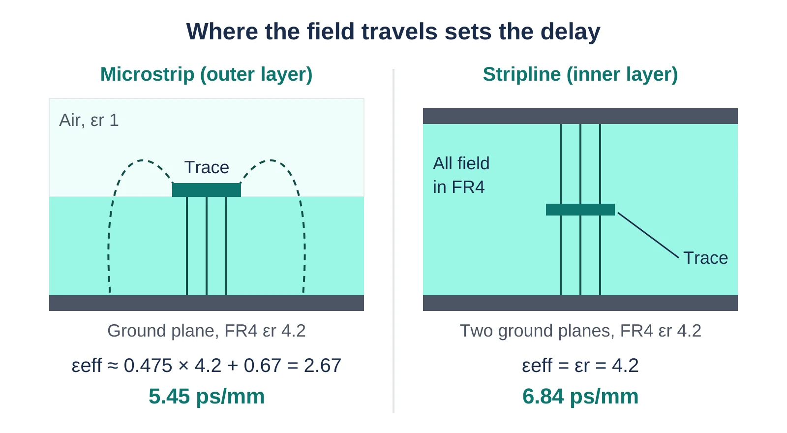
Wikipedia describes the microstrip mode as quasi TEM and notes that its effective dielectric constant climbs gradually toward that of the substrate as frequency rises. So microstrip delay from a field solver at 10 GHz can differ slightly from a low frequency estimate.
Solder mask adds a thin dielectric layer over a microstrip and raises its delay a little. For tight outer layer timing, ask the fabricator for the mask thickness.
How to Calculate Propagation Delay on a PCB
To calculate PCB propagation delay, find εeff for the trace type, take its square root and multiply by 84.73 ps/in, then multiply by the trace length. The constant 84.73 is simply 25.4 mm divided by the speed of light, 0.2998 mm per ps.
Stripline: tpd = 84.73 × √εr ps/in
Microstrip: εeff ≈ 0.475 εr + 0.67
tpd = 84.73 × √εeff ps/in
ps/mm = (ps/in) ÷ 25.4
Total delay = tpd × length
The microstrip formula above is the simple approximation used in Analog Devices MT 094, and it ignores trace geometry. Sierra Circuits uses 0.64 εr + 0.36 for wider traces, which gives about 5.82 ps/mm for the same laminate, so always confirm critical outer layer nets with your fabricator or a field solver.
√4.2 = 2.049
tpd = 84.73 × 2.049 = 173.6 ps/in
173.6 ÷ 25.4 = 6.84 ps/mm
Delay = 6.84 × 100 = 684 ps
Rise time 1 ns: Lc = 1000 ÷ (2 × 6.84) = 73 mm
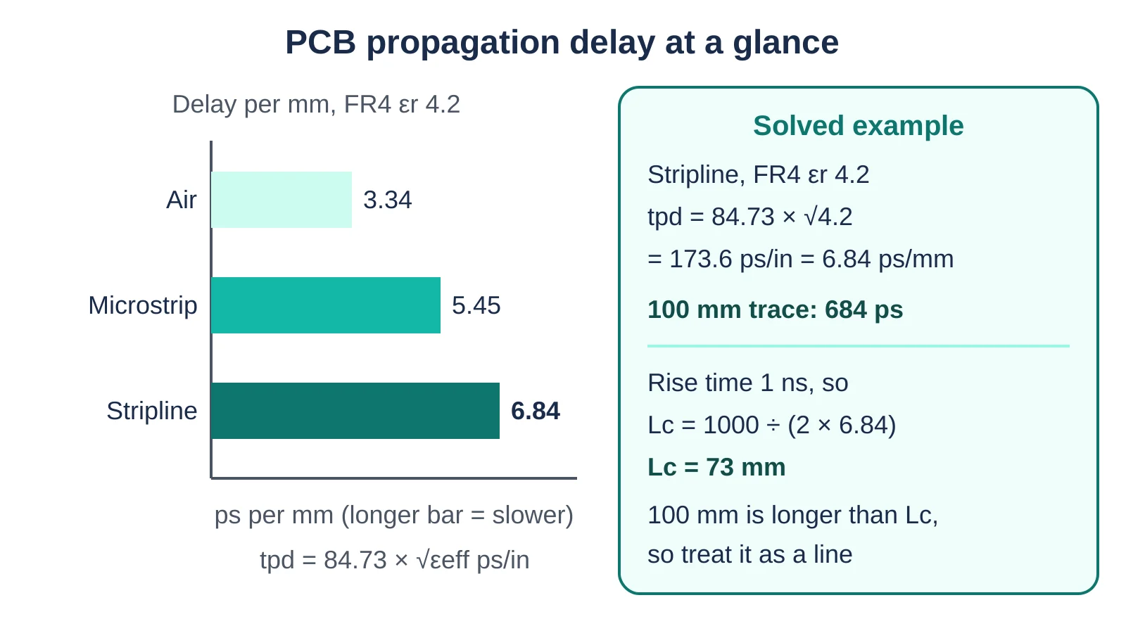
Change the type to 2 and the same 100 mm trace drops to about 545 ps at 5.45 ps/mm, with a critical length near 92 mm. Once you know the delay, size the copper width for current with our PCB trace width calculator and then tune width for impedance in the stackup tool.
Microstrip vs Stripline Propagation Delay
Stripline is always slower than microstrip on the same laminate, because all of its field lines sit inside the dielectric. On FR4 with εr 4.2 the difference is about 1.39 ps per mm, which becomes 139 ps over 100 mm.
| Parameter | Microstrip | Stripline |
|---|---|---|
| Location | Outer layer, air above | Inner layer, planes on both sides |
| εeff at εr 4.2 | About 2.67 (approximation) | 4.2 |
| Delay per inch | About 138.3 ps | About 173.6 ps |
| Delay per mm | About 5.45 ps | About 6.84 ps |
| Signal speed | About 184 mm per ns | About 146 mm per ns |
| Depends on geometry | Yes, slightly | Almost no |
| Shielding and crosstalk | Weaker | Better |
Altium gives typical values of about 150 ps/in for a 50 ohm microstrip and 171 ps/in for stripline on a Dk 4 laminate, which agrees well with the formulas. Your layer stackup design decides which nets go on outer layers and which go inside, so it fixes their delay before routing starts.
A 0.1 mm and a 0.3 mm stripline on the same core have almost the same delay per millimetre, even though their impedance is very different.
What Is Critical Length in PCB Design?
Critical length is the trace length beyond which a digital edge sees the trace as a transmission line, and Analog Devices sets it where one way delay equals half the rise time. Above that length you need controlled impedance traces and termination.
tr = 1 ns = 1000 ps, tpd = 6.84 ps/mm
Lc = 1000 ÷ 13.68 = 73 mm
Analog bandwidth: tr ≈ 0.35 ÷ fmax
The clock frequency is not in the formula, only the edge rate, so a slow clock from fast logic still needs care on long traces. Analog Devices also gives a conservative rule of about 2 inches of trace per ns of rise time, and you can use impedance matching with series or parallel resistors once a net crosses that limit.
Measure the real rise time at the receiver with a fast probe, because many datasheets quote the slowest case. Edges from modern FPGAs and microcontrollers are often far faster than the clock rate suggests.
PCB Propagation Delay in Length Matching for DDR and Clocks
Length matching uses PCB propagation delay to make all bits of a bus arrive inside the same timing window, and the safe way is to match in picoseconds, not millimetres. Modern CAD tools convert a delay rule into length per layer once you enter the stackup.
Millimetres mislead across layers: 50 mm of microstrip takes about 272 ps, while 50 mm of stripline takes about 342 ps, a 70 ps gap for two nets of the same length. If a controller allowed 10 ps of skew, stripline mismatch would need to stay within 10 ÷ 6.84 = 1.46 mm, so take the real budget from the controller layout guide.
For pairs, our guide on differential pair routing explains where to place tuning bumps so the coupling is not broken. Serpentines also couple to themselves and to neighbours, so keep loop spacing wide as described in our article on PCB crosstalk reduction.
- Set the rule in picoseconds and let the tool convert per layer
- Include package pin delay from the chip vendor
- Tune close to the mismatch source
- Keep serpentine gaps at least three trace widths
- Matching only in millimetres across layers
- Ignoring via and connector delay
- Tight serpentines that couple to themselves
- Tuning over a split plane or void
Troubleshooting Skew and Timing Errors
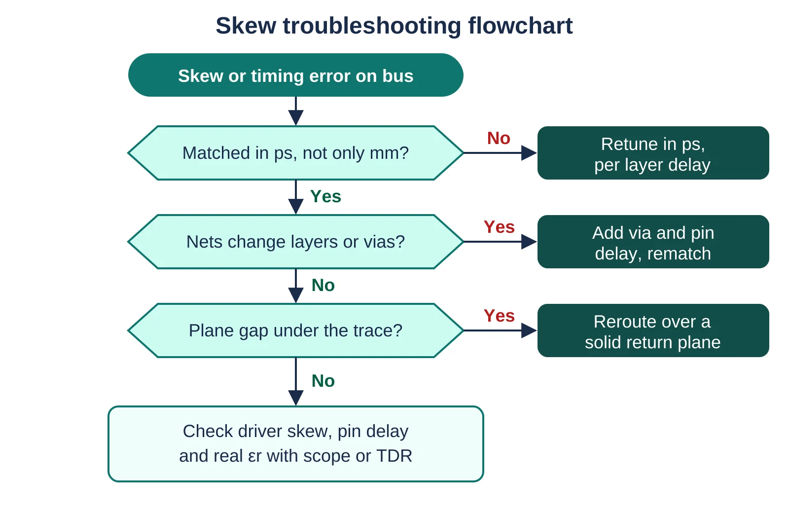
Most skew problems come from matching in the wrong unit, mixing layers, ignoring via and pin delay, or routing over a broken plane. Work through the flowchart below in order, since each check is cheaper than the next.
| Symptom | Likely cause | Field fix |
|---|---|---|
| One bit fails at high data rate | That net changes layer and runs longer in stripline | Rematch in ps using per layer delay |
| Measured delay higher than calculated | Real εr higher than assumed | Use fabricator εr or measure with TDR |
| Pair shows common mode noise | Intra pair skew from uneven bends | Add a small bump near the bend that caused it |
| Ringing on a clock line | Trace longer than critical length without termination | Add a series resistor near the driver |
A broken reference changes both impedance and PCB propagation delay, so check the plane under every timed trace using our guides on ground plane design and the PCB return current path. Vias add delay and a discontinuity, and our article on through hole, blind and buried vias helps you pick the right type.
- Laminate εr taken at the operating frequency
- Delay rules written in ps, not only mm
- Package pin delay included for DDR and FPGA nets
- Solid reference plane under every timed net
- Critical length checked against measured rise time
- Final skew report reviewed after routing
To verify PCB propagation delay in the lab, use a TDR or two deskewed channels on a fast oscilloscope, as covered in our article on the cathode ray oscilloscope. Simultaneous switching can also shift edges in time, so review ground bounce before blaming the trace.
Eric Bogatin explains why a signal is a wave travelling between the trace and its return path, and that is why the dielectric sets the delay.
If you are new to layout, start with these PCB design basics and our list of essential PCB design rules. For outer layer impedance, a microstrip impedance calculator pairs well with the delay numbers here, and our guide on high speed PCB signal integrity goes deeper.
PCB Propagation Delay FAQ
PCB propagation delay is the time an edge needs to travel along a trace, usually quoted in ps/in or ps/mm. On FR4 with εr 4.2 it is about 6.84 ps/mm for stripline and 5.45 ps/mm for microstrip.
Engineers measure it with a TDR or by comparing two scope channels at both trace ends after deskewing the probes.
Stripline is slower because its whole field sits inside the dielectric, while microstrip shares part of its field with air. With εr 4.2, a 100 mm stripline takes about 684 ps and the same microstrip about 545 ps.
That 139 ps gap is why outer and inner layer lengths cannot be matched in millimetres alone.
Take the square root of εr, multiply by 84.73 to get ps per inch, then divide by 25.4 for ps per mm. For εr 4.2 that gives 173.6 ps/in or 6.84 ps/mm.
Multiply by the routed length, so a 100 mm trace gives about 684 ps of one way delay.
A trace behaves like a transmission line when its one way delay is more than half the signal rise time. Critical length is the rise time divided by twice the delay per mm.
With a 1 ns edge on FR4 stripline, that is 1000 ÷ (2 × 6.84), or about 73 mm.
The usual cause is matching in millimetres while nets run on different layers, because microstrip is faster than stripline. Vias, connector pins and package delay inside the chip also add time that a plain length rule ignores.
Set the constraint in picoseconds, include pin delay from the datasheet and recheck the report after routing.
A laminate with lower εr gives lower delay, because delay scales with the square root of the effective dielectric constant. Moving from εr 4.2 to εr 3.0 cuts stripline delay from 6.84 to about 5.78 ps/mm.
Choose by loss, cost and stack availability as well, since delay alone rarely drives material choice.
Related Articles
- Signal Integrity in High Speed PCB Design
- Controlled Impedance PCB Traces
- Differential Pair Routing on PCB
- PCB Layer Stackup Design
- PCB Crosstalk Reduction
External References
- Analog Devices MT 094: Microstrip and Stripline Design (PDF)
- Sierra Circuits: Signal Propagation Delay in PCB
- Wikipedia: Microstrip
What We Learn Today
- PCB propagation delay equals 84.73 × √εeff ps per inch, so FR4 stripline with εr 4.2 gives about 6.84 ps per millimetre of trace.
- Microstrip is faster than stripline because part of its field travels in air, giving about 5.45 ps/mm on the same FR4 laminate.
- A trace longer than rise time divided by twice its delay acts as a transmission line, and bus matching should be written in picoseconds.