
At high speed, a trace stops being a simple wire and becomes a transmission line with its own characteristic impedance.
Controlled impedance means designing and manufacturing PCB traces so their characteristic impedance stays at a specified value, such as 50 Ω. It prevents reflections that distort fast digital and RF signals.

What Is Controlled Impedance?
Controlled impedance is the practice of holding the characteristic impedance of PCB traces within a tolerance, usually plus or minus 10 percent. It treats each trace and its reference plane as a transmission line, a key part of high speed signal integrity.
Sierra Circuits explains that reflections occur whenever impedance changes along a trace. Those reflections cause ringing, overshoot and timing errors.
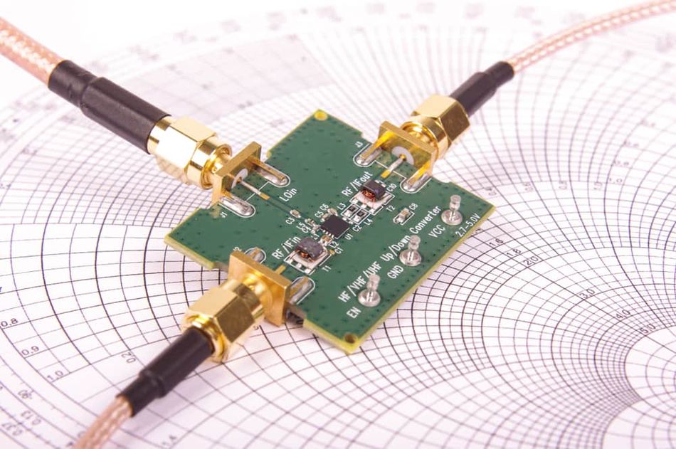
Characteristic impedance is not the same as DC resistance. It depends on inductance and capacitance per unit length, set by geometry and materials.
Common targets are 50 Ω for single ended RF and many digital lines, 90 Ω for USB differential pairs and 100 Ω for Ethernet, HDMI and DDR differential pairs.
5 Crucial Controlled Impedance Stackup Factors
Sierra Circuits adds resin content and glass weave as material factors that shift Dk locally. For very fast links, these details matter.
Plan all these values in the layer stackup with your fabricator. They will adjust widths slightly to hit the target on their process.
IPC 2141 Microstrip Formula With Example
h = dielectric height, w = trace width, t = copper thickness
Worked example, FR4 outer layer:
h = 0.2 mm, w = 0.35 mm, t = 0.035 mm, εr = 4.3
87 ÷ √5.71 = 36.4
5.98 × 0.2 ÷ (0.28 + 0.035) = 3.80, ln = 1.334
Z0 ≈ 48.6 Ω, close to a 50 Ω target
This classic formula is an approximation valid for common geometries. Final values should come from a field solver or the fabricator impedance tool.
Width choices also affect current capacity, so cross check with a PCB trace width calculator for power nets.
When You Need Controlled Impedance
Sierra Circuits suggests impedance becomes critical above about 100 MHz. In practice, rise time matters more than frequency, just as with crosstalk.
Short traces on slow signals do not need control. Adding it everywhere raises cost without benefit.
Terminations match the line to its load, much like the 75 Ω termination on ControlNet networks.
Microstrip vs Stripline Impedance
| Feature | Microstrip | Stripline |
|---|---|---|
| Location | Outer layer | Inner layer between planes |
| Effective Dk | Lower, part air | Full material Dk |
| Signal speed | Faster | Slower |
| Width for 50 Ω | Wider | Narrower |
| Shielding and EMI | Weaker | Better |
Stripline gives better shielding and less crosstalk, while microstrip is easier to probe and rework. Many boards use both.
Via transitions between layers must keep a return path nearby, covered in PCB via types.
Controlled Impedance Design Checklist
TDR testing sends a fast step down the coupon and measures reflections, showing impedance along its length. Fabricators report results with each batch.
For more layout discipline, see our essential PCB design rules guide.
Differential Pair Impedance
A differential pair carries equal and opposite signals on two coupled traces. Its differential impedance depends on each trace impedance and on the coupling between them, so spacing becomes a design variable.
Tighter spacing increases coupling and lowers differential impedance. For controlled impedance pairs, keep width and spacing constant along the whole route, including under connectors and near vias.
Length matching within a pair keeps the two edges aligned. A small serpentine near the source corrects skew without breaking controlled impedance for long.
Microstrip Impedance Calculator
Increase the width and watch impedance fall, or increase height and watch it rise. Use this for quick planning only.
- Clean edges without reflections.
- Reliable high speed interfaces.
- Predictable timing.
- Lower EMI.
- Higher fabrication cost.
- Tighter material and process control.
- Needs test coupons.
- Formulas are only estimates.
TI High Speed Layout Guidelines PDF
PCB Track Impedance With Eric Bogatin
Controlled Impedance FAQ
Related Articles
- PCB Layer Stackup Design
- PCB Trace Width Calculator
- Signal Integrity for High Speed PCB
- What Is Signal Integrity
- Ground Plane PCB Design
External References
- High Speed Interface Layout Guidelines, Texas Instruments
- Why Impedance Control Matters, Sierra Circuits
- Impedance Control Guide, Wevolver
- Microstrip, Wikipedia
What We Learn Today
- Fast signals need traces treated as transmission lines with set impedance.
- Width, height, Dk, copper and plane continuity decide the value.
- Work with the fabricator and verify with TDR coupons.