
When many outputs switch at once, the chip ground itself jumps, and a quiet low output suddenly looks like a logic high.
Fast digital outputs pull sharp current spikes through tiny package and via inductances. The resulting voltage shifts the internal ground of the chip away from the board ground and creates false signals.
What Is Ground Bounce?
Ground bounce is a temporary shift of the internal ground reference of an IC, caused when switching current flows through the inductance of its ground pins, bond wires and vias. The die ground moves relative to the board ground, so outputs that should be low can briefly rise and inputs can be misread, a classic signal integrity problem.
All About Circuits explains that switching current through package inductance, following V = L × di/dt, creates a voltage difference between the PCB ground and the die ground. The faster the edge, the larger the jump.
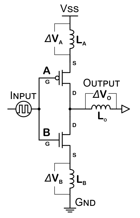
The same effect on the supply pin is called supply bounce or rail collapse. Both happen together when outputs change state.
Every pin, bond wire and via behaves like a small inductor, typically a few nanohenries. At nanosecond edges, that is enough to matter.
How Switching Current Creates the Bounce
All About Circuits also notes that the noise spreads through shared power and ground rails, not only at the gate that switched. Neighbouring logic and analog parts feel it too.
Ringing follows the jump, because the inductance resonates with load and package capacitance. Our noise reduction for digital ICs guide covers related effects.
Measuring it needs a low inductance probe ground, such as a spring tip, and a quiet output held low while the others switch. A long probe ground lead adds its own inductance and exaggerates what the scope shows.
Simultaneous Switching Noise Formula
N = outputs switching together, L = shared ground inductance, ΔI = current change per output, Δt = edge time
Worked example:
8 outputs, 20 mA each, edge 1 ns
Ground path inductance = 5 nH
V = 8 × 5 nH × 0.02 A ÷ 1 ns
Ground bounce ≈ 0.8 V, enough to upset 3.3 V logic
Halving the edge time doubles the bounce, and doubling the number of pins in parallel roughly halves it. That explains why modern packages have so many ground balls.
The old Quality Semiconductor note on TTL logic shows the same trend, with bounce rising sharply as more outputs switch at once.
7 Proven Layout Fixes
Decoupling is the first defence, explained in how decoupling capacitors work. All About Circuits stresses that capacitors close to the IC keep the current loop small.
A continuous plane from the layer stackup gives the lowest inductance return path. See ground plane PCB design for layout rules.
Bounce vs Other Ground Problems
| Problem | Cause | Frequency | Main Fix |
|---|---|---|---|
| Switching bounce | L × di/dt in package and vias | Nanosecond edges | Decoupling and low inductance |
| Ground loop | Multiple ground paths | Mains and low frequency | Single point grounding |
| Crosstalk | Coupling between traces | Fast edges | Spacing and planes |
| Common impedance | Shared return path | Any | Separate returns |
Ground loops are a very different, low frequency issue, covered in ground loop causes and prevention. Do not confuse the fixes.
Via inductance adds directly to package inductance, so via count and length matter, see PCB via types.
Bounce Voltage Calculator
Compare the result with the low level input threshold of the receiving logic, often about 0.8 V. Keep the bounce well below that with margin.
- Decoupling at every supply pin.
- Short, wide ground connections.
- Controlled edge rates.
- Continuous planes under ICs.
- Long lead packages.
- Shared ground vias.
- Wide buses switching together.
- Split planes under fast parts.
Ground Bounce Application Note PDF
Layout Change With Eric Bogatin
Ground Bounce FAQ
Related Articles
- Ground Plane PCB Design
- How Decoupling Capacitors Work
- Signal Integrity for High Speed PCB
- Noise Reduction in Digital ICs
- Essential PCB Design Rules
External References
- Noise in TTL Logic, Quality Semiconductor
- Reducing Switching Noise, All About Circuits
- Ground Bounce, Wikipedia
What We Learn Today
- Ground bounce comes from L × di/dt in package pins and vias.
- More simultaneous outputs and faster edges raise it.
- Close decoupling, solid planes and slower edges keep it small.