
A buck converter steps down a DC input voltage to a lower DC output voltage. It switches a transistor on and off at high frequency. The on/off ratio sets the output voltage.
This guide explains the switching cycle, the duty cycle formula, the role of each component, a fully worked design example, and a live duty cycle calculator.
A linear regulator wastes excess voltage as heat. A buck converter recycles it, achieving efficiencies of 85 to 97 percent.
For any application where a supply must power circuits at a lower voltage, a buck converter is almost always the right choice.
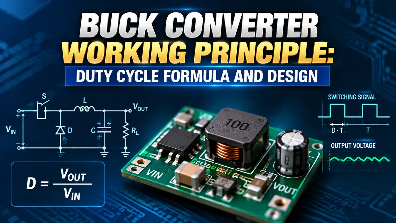
How a Buck Converter Works: The 2-Phase Switching Cycle
A buck converter controls output voltage by repeating two phases thousands of times per second. The ratio of the ON phase to the full period is called the duty cycle.
The boundary between CCM and DCM occurs at the critical inductance: L critical = (Vout x (1 minus D)) / (2 x f x Iload). Choosing an inductance above this value keeps the converter in CCM at the target load current.
The Duty Cycle Formula Explained
Duty cycle (0 to 1). Fraction of each switching period that the MOSFET is ON.
Target output voltage (V). Always lower than Vin in a buck converter.
Input supply voltage (V). The voltage being stepped down.
Switching frequency (Hz). Typically 100 kHz to 2 MHz in modern designs.
The duty cycle formula assumes an ideal converter with zero losses. In a real buck converter, the MOSFET has an on-resistance (RDS(on)), the diode has a forward voltage drop, and the inductor has a DC resistance (DCR). These losses reduce the actual output voltage slightly below D x Vin. The controller compensates by increasing D to maintain the regulated output.
The MOSFET switching characteristics affect the effective duty cycle at high switching frequencies. At 2 MHz, a 10 ns rise time already occupies 2% of the switching period.
Most buck converter controllers impose a minimum on-time and a maximum duty cycle. Operating near these limits reduces regulation quality and increases output ripple. If your duty cycle calculation gives D above 0.9 or below 0.1, choose a different input voltage range or use a different topology.
4 Key Components in a Buck Converter
Live Duty Cycle and Inductor Design Calculator
Worked Example: 12 V to 5 V at 2 A, 300 kHz
Vin = 12 V, Vout = 5 V, Iout = 2 A
Switching frequency f = 300 kHz, ripple ratio = 0.30
Step 1: Duty cycle
D = Vout / Vin = 5 / 12 = 0.417 (41.7%)
Step 2: Target ripple current
ΔIL = ripple ratio x Iout = 0.30 x 2 = 0.60 A peak-to-peak
Step 3: Minimum inductance
L = (Vin minus Vout) x D / (f x ΔIL)
L = (12 minus 5) x 0.417 / (300000 x 0.60)
L = 7 x 0.417 / 180000 = 2.917 / 180000 = 16.2 µH
Select standard value: 22 µH (next value above, gives lower ripple than spec)
Step 4: Peak inductor current (for saturation rating)
Ipeak = Iout + ΔIL/2 = 2 + 0.30 = 2.30 A
Select inductor with saturation current above 2.30 A with margin (e.g. 3 A rated)
Step 5: Critical inductance (CCM/DCM boundary at 2 A load)
Lcrit = Vout x (1 minus D) / (2 x f x Iout)
Lcrit = 5 x 0.583 / (2 x 300000 x 2) = 2.917 / 1200000 = 2.43 µH
Selected 22 µH is well above 2.43 µH: converter stays in CCM at full load
Step 6: Efficiency estimate (90% typical for this design)
Pin = Vout x Iout / efficiency = 5 x 2 / 0.90 = 11.1 W
Power dissipated as heat: 11.1 minus 10 = 1.1 W
5-Step Buck Converter Design Checklist
Define the specification: Vin range, Vout, Iout max, efficiency target
Use the worst-case Vin (minimum input) to calculate maximum duty cycle D max = Vout / Vin min. This is the critical operating point for inductor and MOSFET selection.
Use the maximum Vin to check that D min is above the controller's minimum on-time limit.
Choose switching frequency: higher frequency means smaller L and Co but lower efficiency
Higher switching frequency reduces inductance and capacitance values but increases MOSFET switching losses. A practical range is 100 kHz to 500 kHz for most designs.
Above 1 MHz is used in portable designs where small board area is the priority.
Use the decoupling capacitor guide to understand output capacitor selection.
Calculate inductance for target ripple current (20 to 40 percent of Iout)
Use L = (Vin minus Vout) x D / (f x ΔIL). A ripple current ratio of 30 percent of Iout is a good starting point. Lower ripple needs a larger inductor.
Higher ripple reduces inductor size but increases output ripple voltage and the risk of DCM at light loads.
Select components: MOSFET for low RDS(on), inductor above Ipeak saturation current
The MOSFET must withstand Vin plus ringing transients (use 1.3x Vin as the minimum voltage rating). The inductor saturation current rating must exceed Ipeak.
An inductor that saturates will lose its inductance and the ripple current will spike. See the MOSFET working principle guide for selection criteria.
Verify thermal performance: MOSFET and inductor must stay below their rated temperatures
Calculate MOSFET conduction loss: P = D x Iout squared x RDS(on). Total MOSFET power dissipation must stay below P max = (Tj max minus Tambient) / Rth(ja).
For the inductor, calculate I squared x DCR loss and verify the inductor body temperature does not exceed its rated value at maximum load.
Steady-state regulation tells you the output voltage at one load point. A load transient test shows how quickly the control loop responds to a sudden load step (for example, from 0 A to full load in 1 microsecond). A slow control loop causes the output voltage to undershoot or overshoot. Test with the fastest expected load step in your system.
Buck Converter vs Linear Regulator: When to Choose Each
| Parameter | Buck Converter | Linear Regulator (LDO) |
|---|---|---|
| Efficiency | 85 to 97 percent. Loss is almost independent of Vin minus Vout. | (Vout / Vin) x 100 percent. Large Vin minus Vout wastes power as heat. |
| Output ripple | 10 to 100 mV typical. Depends on switching frequency and capacitor ESR. | Essentially zero ripple. Suitable for noise-sensitive analog circuits. |
| Complexity | Controller IC, MOSFET, inductor, diode, capacitors. More components and layout care required. | Input cap, output cap, feedback resistors. Very simple design. |
| PCB area | Larger at low frequency. Shrinks to a few mm squared at 2 MHz with integrated solutions. | Very small. Often a single IC with two capacitors. |
| EMI | Generates switching EMI. Requires careful PCB layout and sometimes input filtering. | No switching. Very low EMI. |
| Best for | Any design where Vin minus Vout is more than 1 to 2 V and load current exceeds 100 mA. | Post-regulation after a buck, noise-sensitive ADC supplies, simple low-current rails. |
Watch: Buck Converter Working Principle Explained
Buck Converter Questions Engineers Ask
Related Articles on This Site
- What Is a MOSFET? Working Principle Explained
- Inductor Working Principle
- How Decoupling Capacitors Work
- Active, Reactive and Apparent Power Explained
- What Is a Semiconductor?
External References
- Basic Calculation of a Buck Converter's Power Stage | Texas Instruments SLVA477B
- Buck Regulator Design Guide | Analog Devices
What We Learn Today
- A buck converter steps down DC voltage by switching a MOSFET on and off. The duty cycle D = Vout/Vin sets the output voltage. A 12 V to 5 V converter runs at D = 41.7 percent.
- The inductor minimum value is L = (Vin minus Vout) x D / (f x ΔIL). The inductor saturation current rating must exceed Ipeak = Iout plus ΔIL/2. These two checks prevent inductor saturation and DCM at full load.
- A buck converter achieves 85 to 97 percent efficiency because energy is stored in the inductor, not wasted as heat. A linear regulator's efficiency equals Vout/Vin and drops sharply with large input-to-output voltage differences.