
Every sensor reading a microcontroller understands started life as a smooth analog voltage. Here is exactly how an ADC turns that into digital numbers, with real Analog Devices architecture diagrams and a live sampling and quantization simulator you can try now.
What Is an ADC?
An analog-to-digital converter, or ADC, translates a continuous, infinitely variable analog signal into a finite set of digital numbers a processor can actually work with.
Every ADC performs two genuinely separate jobs: sampling, which captures the signal at discrete moments in time, and quantization, which rounds each captured value to the nearest available digital code. Both steps introduce their own hard limits, and understanding those limits is most of what it takes to design a working data acquisition system.
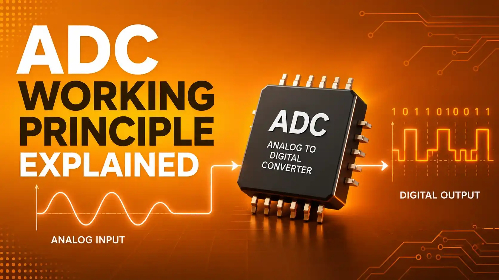
That digital output often feeds straight into a register built from flip-flop types like the ones we covered previously, or gets routed through logic covered in our encoder vs decoder guide.
This guide covers the five essential facts behind the ADC working principle, from the Nyquist criterion that governs sampling to the real architecture trade-offs between speed and resolution. Getting comfortable with the ADC working principle pays off well beyond any single project, since nearly every modern sensor and instrument depends on it.
How the ADC Converts a Signal
Every ADC, regardless of internal architecture, follows the same four-stage sequence to turn a voltage into a number.
Analog Signal Arrives
A continuous, infinitely variable voltage enters the ADC's input, carrying real-world information.
Sampling Captures Time Snapshots
The signal is measured at uniform, discrete time intervals set by the sampling clock.
Quantization Assigns a Level
Each captured sample is rounded to the nearest of a finite set of discrete digital levels.
Binary Code Is Output
That quantized level is output as a binary code a processor can store, compare, or transmit.
5 Essential Facts About the ADC
These five facts about the ADC working principle explain almost every practical question that comes up when selecting or designing around a converter.
Sampling and Quantization Are Two Separate Processes
Sampling limits resolution in time, quantization limits resolution in amplitude. Each introduces its own distinct error, and both must be understood together to predict real ADC performance.
The Nyquist Criterion Sets the Sampling Rate Floor
The sampling rate must exceed twice the highest frequency component in the input signal. Sample any slower, and higher frequencies fold back into the signal band as aliasing, corrupting the result permanently.
Resolution Sets the Number of Discrete Levels
An N-bit ADC produces exactly 2^N possible output codes. More bits mean finer steps, but quantization error, the rounding between those steps, never fully disappears no matter how many bits you add.
SNR and ENOB Reveal Real-World Performance
A real converter's actual dynamic performance, including noise and distortion, is captured by its effective number of bits, which is often lower than its stated resolution suggests.
No Single ADC Architecture Wins Everywhere
Flash, SAR, sigma-delta, and pipeline architectures each trade speed against resolution differently, which is exactly why so many distinct ADC families exist side by side.
The Nyquist Criterion in the ADC Working Principle
Sampling too slowly does not simply blur a signal, it permanently disguises high frequencies as false low frequencies.
SAR ADC Architecture
The successive-approximation-register, or SAR, converter narrows down the answer step by step, much like a balance scale testing progressively smaller weights.
What is happening: The SAR logic compares the input against a series of successively smaller reference voltages, one bit at a time, starting with the most significant bit.
A real example: An 8-bit SAR ADC needs exactly 8 comparison cycles to fully resolve one sample, regardless of the input value, giving it a predictable, fixed conversion time.
Why it works: Using only a single comparator to achieve high resolution keeps the chip small and low power, which is exactly why SAR converters dominate general-purpose sensor and data acquisition applications.
SNR and ENOB Formulas
Two related formulas describe how close a real ADC comes to its theoretical ideal performance.
Ideal SNR: SNR = 6.02N + 1.76 dB
Effective bits: ENOB = (SINAD − 1.76) / 6.02
Worked example: 12-bit ADC, ideal case
SNR = 6.02(12) + 1.76 = 73.98 dB
Worked example: same ADC, measured SINAD = 68 dB
ENOB = (68 − 1.76) / 6.02 = 11.0 effective bits
That 1-bit gap between the stated 12-bit resolution and the measured 11.0 effective bits is completely normal. Real noise, distortion, and non-idealities always eat into a converter's theoretical performance by some amount.
Try It: Sampling and Quantization Simulator
Pick a resolution and a sampling rate to see the ADC working principle in action on a smooth analog wave.
ADC Architecture Comparison
Click each tab to see how the major implementations of the ADC working principle actually differ in practice.
A flash ADC uses 2^N-1 comparators running in parallel, converting in a single clock cycle. It is the fastest architecture available, but practical resolution is generally limited to around 8 bits due to the sheer number of comparators needed.
A SAR ADC uses just one comparator and resolves one bit per clock cycle, trading some speed for a much smaller, lower-power design. It dominates general-purpose sensor and instrumentation applications.
A sigma-delta ADC oversamples the input at a much higher rate using a simple 1-bit modulator, then relies on digital filtering to extract very high resolution. It excels at precision, low-bandwidth measurements like weigh scales and audio.
A pipeline ADC splits the conversion across several stages, each resolving a few bits and passing the remainder onward. It balances speed and resolution well but introduces a fixed latency called pipeline delay.
ADC Architecture Comparison Table
| Architecture | Typical Speed | Typical Resolution | Best For |
|---|---|---|---|
| Flash | Very fast, 1 clock cycle | Up to about 8 bits | High-speed digitizers, oscilloscopes |
| SAR | Moderate, N clock cycles | 8 to 18 bits | General-purpose sensors, data acquisition |
| Sigma-Delta | Slower, oversampled | 16 to 24 bits | Precision measurement, audio, weigh scales |
| Pipeline | Fast, with latency | 8 to 16 bits | Video, wideband IF sampling |
Applications of ADCs
Sensor Data Acquisition
Temperature, pressure, and level sensors all rely on an ADC to digitize their output.
Audio Recording
Microphones produce an analog voltage that must be sampled and quantized to store digitally.
Digital Oscilloscopes
High-speed flash or pipeline ADCs capture waveforms fast enough to display in real time.
Medical Imaging
Precision sigma-delta converters digitize the faint signals behind ECG and ultrasound systems.
Industrial Process Control
SAR ADCs convert 4 to 20mA loop signals into readings a PLC can process.
Software-Defined Radio
High-speed ADCs digitize RF signals directly for processing entirely in software.
Advantages and Limitations of ADCs
Why Digitizing a Signal Pays Off
Limitations to Keep in Mind
Download ADC References
These two official references go deeper into the ADC working principle, sampling theory, and architecture selection.
MT-002: What the Nyquist Criterion Means to Your Sampled Data System Design
Official Analog Devices tutorial on sampling theory and aliasing
SAR and Delta-Sigma ADCs: Understanding Basic Operation
Official Texas Instruments precision labs presentation comparing architectures
Watch: ADC Sampling, Quantization, and Encoding Explained
This video walks through the ADC working principle from sampling through encoding.
FAQs on the ADC Working Principle
These questions cover the details of the ADC working principle that come up most often in real design work.
External References
- Analog Devices, MT-002: What the Nyquist Criterion Means to Your Sampled Data System Design
- Analog Devices Wiki, Chapter 20: Analog to Digital Conversion
- Texas Instruments, SAR and Delta-Sigma ADCs: Understanding Basic Operation
- YouTube, Analog to Digital Conversion Explained: Sampling, Quantization and Encoding
What we learn today
- An ADC performs two separate jobs, sampling in time and quantization in amplitude, each with its own limits.
- The Nyquist criterion requires sampling above twice the highest input frequency, or aliasing permanently corrupts the result.
- Resolution sets the number of discrete levels, but quantization error never fully disappears regardless of bit depth.
- SNR and ENOB reveal a converter's real-world performance, which is usually a bit lower than its stated resolution alone suggests.
- Flash, SAR, sigma-delta, and pipeline architectures each trade speed against resolution differently, which is why all four still exist today.