The inverting op amp stage is the first circuit most students build and the one engineers use every day for scaling, summing and filtering. Two resistors set its gain, but bandwidth, output swing and resistor choice decide whether it really works.
Inverting amplifier gain depends only on the ratio of two resistors when the op amp is close to ideal. This guide derives the formula, explains virtual ground and input impedance, and shows how bandwidth and supply limits affect a real design.
What Is Inverting Amplifier Gain?
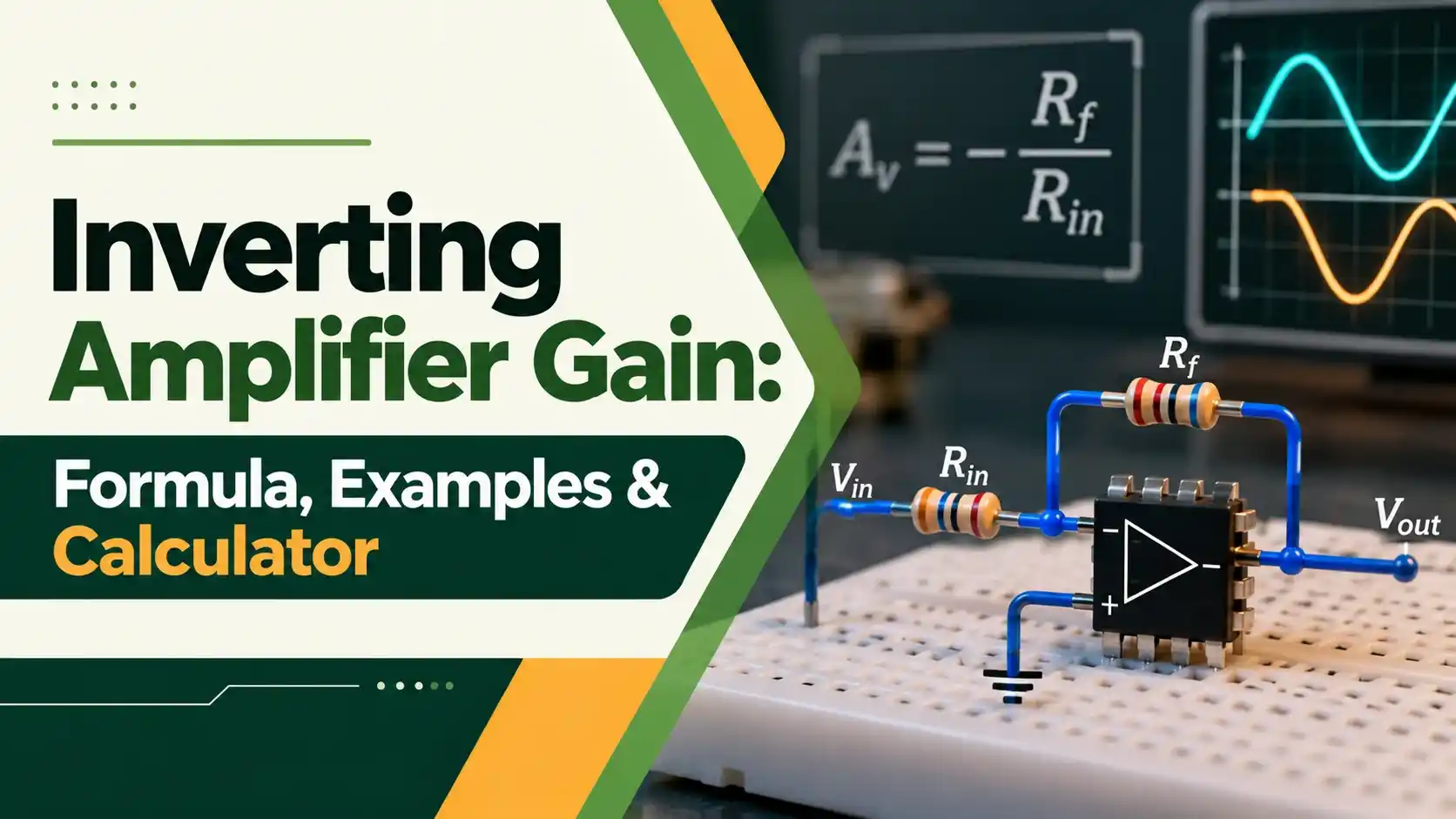
Inverting amplifier gain is the ratio of output voltage to input voltage in an op amp stage where the signal enters the inverting input through Rin and a resistor Rf feeds the output back to the same input. For an ideal op amp it equals minus Rf divided by Rin, so the output is Rf/Rin times larger and shifted by 180°.
- Inverting amplifier gain: Av = minus Rf ÷ Rin.
- Rf = 100 kΩ and Rin = 10 kΩ give a gain of minus 10, or 20 dB.
- The inverting input sits at virtual ground, about 0 V.
- Input impedance is simply Rin.
- Bandwidth = GBW ÷ (1 + Rf/Rin), not GBW ÷ gain.
The minus sign does not mean the signal is made smaller. It only means the output moves in the opposite direction to the input, so a positive input gives a negative output.
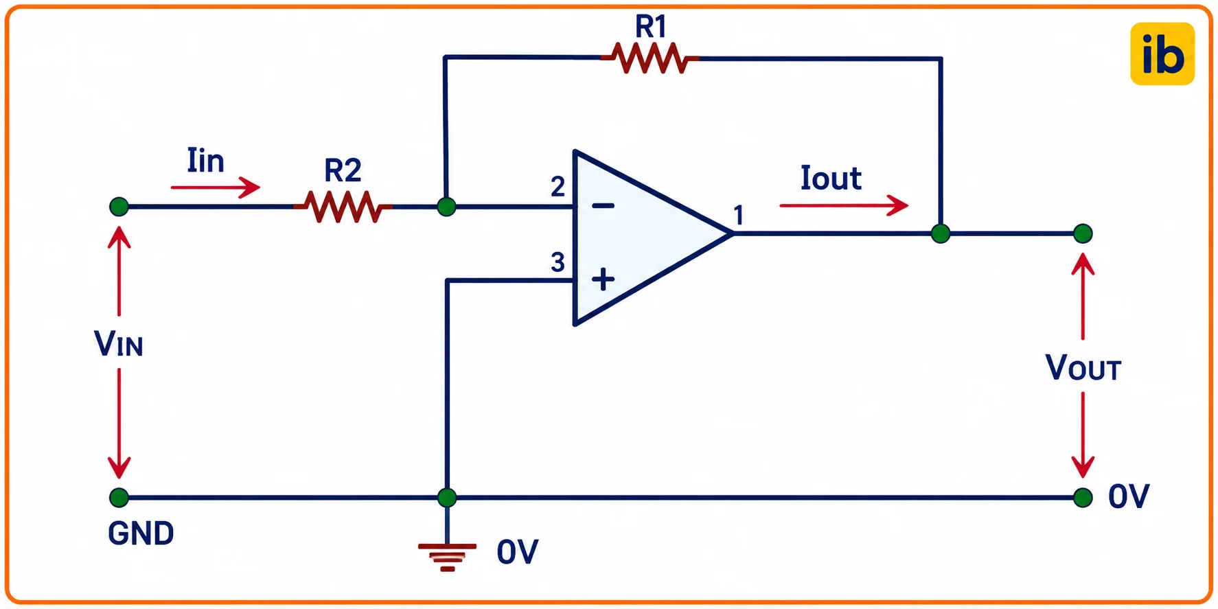
In the circuit above the non inverting input is tied to ground, the input resistor carries the signal to the inverting input and the feedback resistor closes the loop. Circuit Digest labels them R2 and R1, so check the names before using any formula.
Inverting Amplifier Gain Formula Derivation
The derivation uses two ideal op amp rules: no current flows into the inputs, and with negative feedback the two inputs sit at the same voltage. Applying Kirchhoff current law at the inverting input then gives the result in three lines.
Same current through Rf: I = (0 minus Vout) ÷ Rf
Equate: Vin ÷ Rin = minus Vout ÷ Rf
Av = Vout ÷ Vin = minus Rf ÷ Rin
Gain in dB = 20 × log10(Rf ÷ Rin)
Because the open loop gain of a real op amp is very large, the error from this ideal result is tiny. With the exact expression Av = minus (Rf/Rin) ÷ (1 + (1 + Rf/Rin) ÷ Aol), a 741 class part with an open loop gain of about 200000 at a gain of 10 is off by only about 0.006 percent.
The inverting stage can have a gain magnitude below 1, which a non inverting stage cannot. With Rf = 4.7 kΩ and Rin = 10 kΩ, the gain is minus 0.47, a handy way to attenuate and invert a signal at the same time.
Virtual Ground and Input Impedance
With the non inverting input grounded and negative feedback active, the op amp drives its output until the inverting input is also at 0 V. That node is called a virtual ground because it stays at ground potential without being connected to ground, and it draws no current into the op amp.
Since the inverting input is at 0 V, the signal source sees only Rin to ground, so the input impedance equals Rin. This is the main weakness of the stage: a 10 kΩ input resistor loads a high impedance source, which is why a voltage follower is often placed in front.
When you probe a working inverting stage with a DMM, the inverting input should read within a few millivolts of 0 V. If it reads volts, the feedback loop is broken or the output is saturated.
Solved Example 1: Inverting Amplifier Gain of Minus 10
Av = minus 100 ÷ 10 = minus 10
Gain in dB = 20 × log10(10) = 20 dB
Vout = minus 10 × 0.2 = minus 2.0 V
Op amp GBW = 1 MHz
Noise gain = 1 + 100 ÷ 10 = 11
Bandwidth = 1 MHz ÷ 11 = 90.9 kHz
The inverting amplifier gain of minus 10 gives a 2 V output that is negative, exactly as predicted. Notice that the bandwidth uses 11 and not 10, a detail that many students miss in exams and designs.
Inverting Amplifier Gain Calculator
Inverting Amplifier Gain and Bandwidth
Analog Devices tutorial MT 033 defines noise gain as 1 + R2/R1 and notes that it is the same for inverting and non inverting stages. The closed loop bandwidth equals the gain bandwidth product divided by this noise gain, not by the signal gain.
The same tutorial gives a sizing example: a closed loop gain of 10 with 100 kHz bandwidth needs at least 1 MHz GBW. It then advises a safety factor of at least 5, so a 5 MHz part would be chosen in practice.
| Inverting Gain | Noise Gain | Bandwidth with 1 MHz GBW |
|---|---|---|
| Minus 1 | 2 | 500 kHz |
| Minus 2 | 3 | 333 kHz |
| Minus 5 | 6 | 167 kHz |
| Minus 10 | 11 | 90.9 kHz |
| Minus 100 | 101 | 9.9 kHz |
This is why a unity gain inverter has only half the bandwidth of a unity gain follower using the same op amp. Phase margin also follows noise gain, as you can see on a Bode plot of the loop.
Solved Example 2: Output Swing and Slew Rate
A sensor gives 1.5 V peak AC, and you want an inverted signal on a plus and minus 12 V supply with a 741 class op amp. A first try with Rin = 4.7 kΩ and Rf = 47 kΩ gives minus 10, so the output would need 15 V peak, beyond the supply.
Choose Rf = 22 kΩ, Rin = 4.7 kΩ
Av = minus 22 ÷ 4.7 = minus 4.68
Vout peak = 4.68 × 1.5 = 7.02 V, safely below 10.5 V
Slew rate SR = 0.5 V/µs
Full power bandwidth = SR ÷ (2π × Vp)
= 500000 ÷ (6.283 × 7.02) ≈ 11.3 kHz
So this stage can deliver a full 7 V peak sine only up to about 11.3 kHz, even though its small signal bandwidth is much higher. For audio or fast sensor signals, choose an op amp with a higher slew rate or reduce the output amplitude.
Inverting vs Non Inverting Amplifier
| Property | Inverting | Non Inverting |
|---|---|---|
| Gain formula | Minus Rf ÷ Rin | 1 + Rf ÷ Rin |
| Phase shift | 180° | 0° |
| Input impedance | Equal to Rin | Very high |
| Minimum gain magnitude | Can be below 1 | At least 1 |
| Common mode voltage | Stays at 0 V | Follows the input |
| Summing several inputs | Easy, virtual ground | Not practical |
The inverting stage wins when you need attenuation, summing or very low common mode error, because its inputs never move. The non inverting stage wins when the source is weak, and the differential amplifier combines both ideas to reject common mode noise.
Since both inputs stay at 0 V, an inverting stage avoids the common mode errors that limit a non inverting stage. That makes it a favourite for precision summing and filtering in measurement circuits.
How to Choose Rf and Rin for the Right Inverting Amplifier Gain
Circuit Digest suggests about 4.7 kΩ to 10 kΩ for the input resistor and around 100 kΩ for the feedback resistor. Very small values load the op amp output, while values in megohms add thermal noise and make bias current errors worse, a point covered in our guide to the instrumentation amplifier.
Use 1 percent metal film resistors, because the gain error is roughly the sum of both tolerances, up to about 2 percent. A small capacitor across Rf adds a low pass corner at 1 ÷ (2π Rf Cf), exactly like an RC low pass filter, and also tames noise.
For a gain of minus 10 with good E96 values, use 10.0 kΩ and 100 kΩ, or 4.99 kΩ and 49.9 kΩ. Matched resistor arrays keep the ratio accurate over temperature even when absolute values drift.
Applications of the Inverting Stage
The op amp integrator is simply an inverting stage with a capacitor in place of Rf. The same virtual ground idea also appears in precision rectifiers and in the input stage of many ADC drivers.
Myths About Inverting Amplifier Gain
Troubleshooting an Inverting Op Amp Stage
| Symptom | Likely Cause | Check |
|---|---|---|
| Output stuck near a rail | Open Rf or input overload | Measure the inverting input voltage |
| Gain lower than expected | Wrong resistor or source loading | Measure Rin, Rf and source impedance |
| Output clipped | Supply too low for the gain | Reduce gain or raise supply |
| Oscillation | Long feedback trace or capacitive load | Add Cf across Rf or isolate the load |
| DC offset at output | Bias current or offset voltage | Add the compensation resistor |
- Gain set by a simple resistor ratio.
- Inputs stay at 0 V, so no common mode error.
- Gain can be below 1 for attenuation.
- Easy to sum many signals.
- Input impedance limited to Rin.
- Output is phase inverted.
- Bandwidth lower than a follower at unity gain.
- Needs a split supply or bias for AC signals.
- Gain magnitude equals Rf/Rin within resistor tolerance.
- Inverting input reads close to 0 V in operation.
- Peak output stays inside the op amp swing.
- Bandwidth from GBW and noise gain meets the signal need.
- Full power bandwidth covers the highest signal frequency.
- Bypass capacitors fitted close to the supply pins.
Use this checklist before you lay out a board, and confirm the result on the bench with an oscilloscope. Our comparator and Sallen Key filter guides show how the same op amp behaves in other configurations.
Analog Devices Gain and Bandwidth Tutorial
Video on the Inverting Op Amp and Virtual Ground
Inverting Amplifier Gain FAQ
The ideal gain is minus Rf divided by Rin, where Rf is the feedback resistor and Rin the input resistor. With 100 kΩ and 10 kΩ the gain is minus 10.
The minus sign shows that the output is inverted. The magnitude depends only on the resistor ratio as long as the op amp has enough open loop gain.
The signal enters the inverting input, so the op amp drives its output in the opposite direction to hold that input at zero volts. A positive input therefore produces a negative output.
For a sine wave this is a 180° phase shift. The size of the output is still set by the ratio of the feedback and input resistors in the circuit.
It is the inverting input node, which stays at almost 0 V because negative feedback forces both inputs to the same voltage. The non inverting input is grounded, so the inverting input follows it.
It is called virtual because no wire joins it to ground. No current flows into the op amp there, so all the input current passes through the feedback resistor.
The input impedance equals the input resistor, because the far end of that resistor sits at virtual ground. A 10 kΩ input resistor gives about 10 kΩ input impedance.
This can load weak sources such as sensors or high impedance probes. Add a buffer stage or raise both resistors in the same ratio when this becomes a problem.
Yes, simply make the feedback resistor smaller than the input resistor, and the output becomes smaller than the input. With 4.7 kΩ feedback and 10 kΩ input, the gain is minus 0.47.
This is a useful way to attenuate and invert a signal in one stage. A non inverting stage cannot do this, because its minimum possible gain is exactly one.
An inverting stage has a gain of minus Rf over Rin and input impedance equal to Rin. A non inverting stage has a gain of 1 plus Rf over Rin and a very high input impedance.
The inverting stage shifts phase by 180° and keeps both inputs at zero volts. The non inverting stage keeps the phase but its inputs follow the signal.
Closed loop bandwidth equals the gain bandwidth product divided by the noise gain, which is 1 plus Rf over Rin. Higher gain therefore means lower bandwidth.
With a 1 MHz op amp, a gain of minus 10 gives about 90.9 kHz bandwidth. A gain of minus 100 drops this to roughly 9.9 kHz, so plan your op amp choice early.
Related Articles
- Operational Amplifier Op Amp Basics
- Voltage Follower Unity Gain Buffer Explained
- Differential Amplifier Basics and CMRR
- Op Amp Integrator and Differentiator
- Bode Plot Gain and Phase Margin
External References
- MT 033 Voltage Feedback Op Amp Gain and Bandwidth, Analog Devices
- Inverting Operational Amplifier, Circuit Digest
- Operational Amplifier Applications, Wikipedia
What We Learn Today
- Inverting amplifier gain equals minus Rf divided by Rin, so two resistors set both the gain magnitude and the 180° phase inversion.
- The inverting input sits at virtual ground, which makes the input impedance equal to Rin and keeps common mode error close to zero.
- Closed loop bandwidth equals the op amp GBW divided by the noise gain 1 + Rf/Rin, while slew rate limits large output swings.