
A plain rectifier and capacitor sip current in sharp spikes, and a boost stage can reshape that current into a clean sine wave.
Most power supplies start with a bridge rectifier and a bulk capacitor, which draw current only near the voltage peaks. Power factor correction forces the input current to follow the voltage, cutting harmonics and wasted current.
What Is a PFC Circuit?
A PFC circuit is a power factor correction stage placed after the input rectifier of a power supply that shapes the input current into a sine wave in phase with the mains voltage. The most common form is an active boost converter, which builds on the boost converter working principle.
Without correction, a diode rectifier feeding a large capacitor draws narrow current pulses near each voltage peak. The power factor then falls to about 0.5 to 0.7 and harmonic distortion is very high.
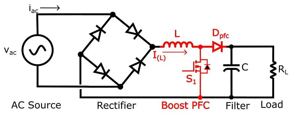
All About Circuits notes that a boost PFC stage needs only a switch, usually a MOSFET, a diode and an inductor. The controller varies the duty cycle so the average inductor current follows the rectified sine voltage.
The same power factor idea used in plants, explained in power factor, kW, kVA and kVAR, applies here, but the problem is distortion rather than phase shift.
How the Boost PFC Circuit Works
Because the boost output must stay above the peak input, the DC bus sits around 390 V to 400 V for universal input. A second converter then steps this down to the required output.
The switch is driven by a gate driver, and fast recovery or silicon carbide diodes reduce losses at turn off. The switching device itself is covered in MOSFET working principle.
3 Boost PFC Circuit Modes
Continuous conduction, inductor current never reaches zero.
Critical conduction, current falls to zero each cycle before the next pulse.
Discontinuous conduction with fixed frequency.
The Infineon design guide uses CCM for its 1200 W example because it keeps peak currents low. Lower ripple current means smaller input filters at high power.
CRM designs switch at zero current, which removes diode reverse recovery loss. The price is variable frequency and higher peak currents.
Power Factor and Input Current Formula
I input rms = P out ÷ (η × V rms × PF)
With PFC: THD 10 percent, cos φ 0.995
PF = 0.995 ÷ 1.005 = 0.990
1200 W, η 0.95, 230 V: I = 5.55 A
Without PFC: THD 100 percent, cos φ 0.95
PF = 0.95 ÷ 1.414 = 0.67, I = 8.2 A
PFC cuts input current by about one third
All About Circuits reports its example reaching a power factor just under 0.99 with about 10 percent THD. That is enough for IEC 61000 3 2 limits and 80 Plus efficiency programs.
The link between distortion and wasted current is explained in THD calculation and power harmonics.
Passive vs Active PFC
| Feature | Passive PFC | Active PFC |
|---|---|---|
| Parts | Large 50 Hz inductor | Switch, diode, small inductor, controller |
| Power factor | About 0.7 to 0.85 | 0.95 to 0.99 |
| Input range | Often switch selected | Universal 90 V to 264 V |
| Size and weight | Heavy | Compact |
| Cost | Low | Higher |
Passive correction still appears in low cost products, but an active PFC circuit dominates above 75 W. Regulations in many regions require it.
A totem pole bridgeless PFC circuit removes the input bridge losses and reaches efficiencies near 99 percent with GaN or SiC switches.
Design Checklist
Bulk capacitor ripple current and ESR decide its life, much like in any switching supply. A UPS input stage uses the same PFC circuit arrangement.
Input Current Calculator
Set THD to 100 percent and cos φ to 0.95 to see a supply without correction. The extra current heats wiring and fills breaker capacity.
- Power factor near unity.
- Low input harmonics.
- Universal input voltage.
- Stable high voltage bus.
- Extra switching losses.
- EMI filtering needed.
- More components and cost.
- High voltage design care.
Infineon PFC Design Guide PDF
How Boost PFC Works Video
PFC Circuit FAQ
Related Articles
- Boost Converter Working Principle
- Power Factor Correction Explained
- Flyback Converter Working Principle
- Buck Converter Working Principle
- THD Calculation
External References
- CCM Boost Design Guide, Infineon
- How the Boost Converter Improves Power Quality, All About Circuits
- Power Factor, Wikipedia
What We Learn Today
- A boost PFC circuit shapes input current to follow the mains voltage.
- CCM suits high power and CRM suits lower power supplies.
- Higher PF cuts input current, harmonics and wiring losses.