
A battery that starts above your output voltage and ends below it needs a converter that can both step up and step down without flipping polarity. The SEPIC topology does exactly that with one switch, two inductors and a coupling capacitor in a simple layout.
Many battery and automotive circuits must hold a steady output while the input wanders above and below it. A SEPIC converter solves that with a positive output, a grounded switch and true shutdown isolation.
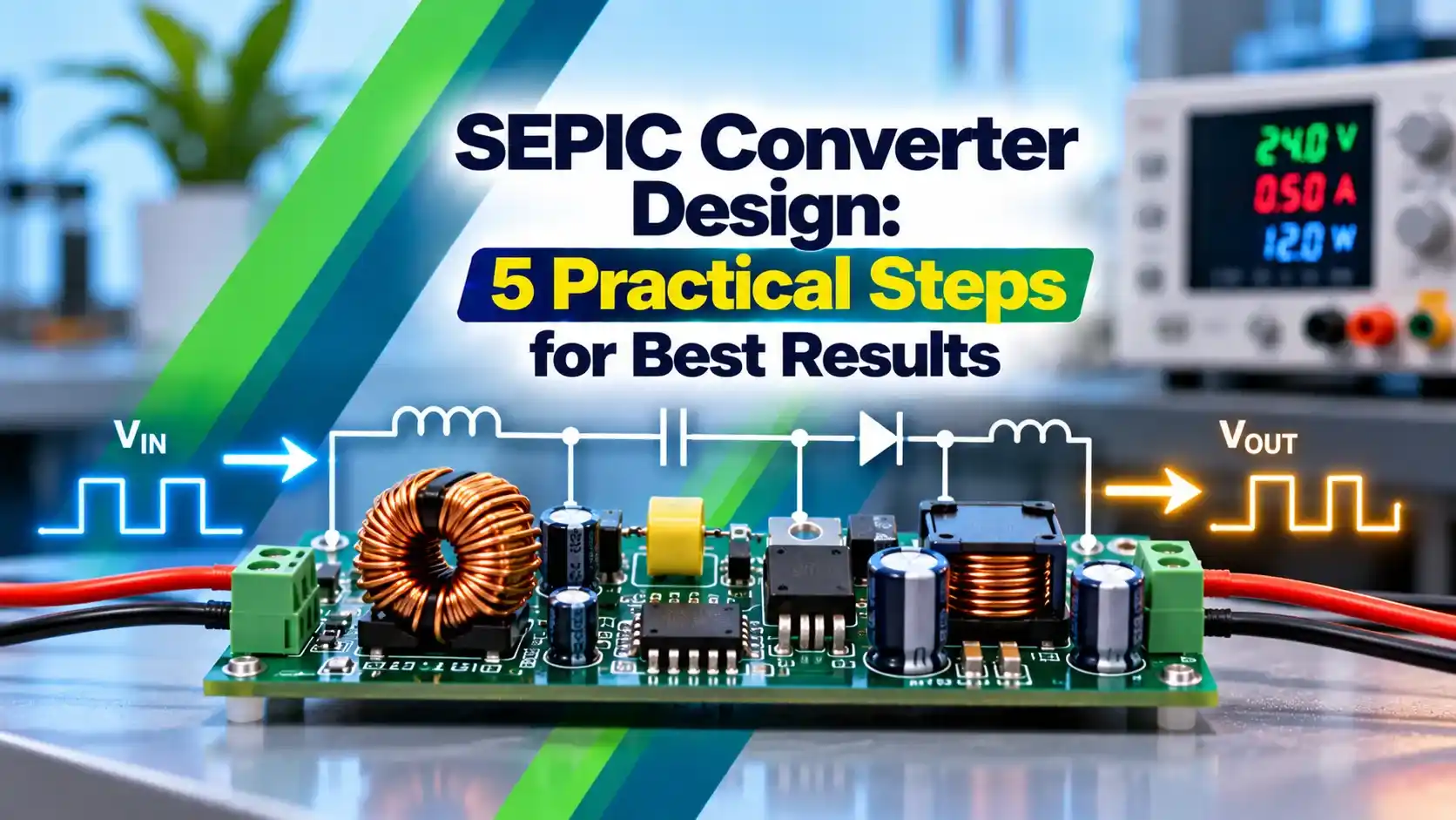
What Is a SEPIC Converter?
A SEPIC converter, short for single ended primary inductor converter, is a DC to DC switching converter whose output can be higher than, lower than or equal to its input, with the same polarity. It builds on the boost converter by adding a second inductor and a series coupling capacitor.
Unlike the classic inverting buck boost, the output is positive with respect to the common ground. Unlike a buck converter, it can keep running when the input falls below the output, which makes it ideal for single cell lithium and car battery circuits.
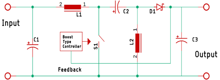
The SEPIC converter circuit has a low side switch, an input inductor L1, a coupling capacitor Cp, a second inductor L2 to ground, an output diode and an output capacitor. Because Cp sits in series, the input and output are isolated in DC terms, so the output falls to zero when the switch stops.
The coupling capacitor in a SEPIC converter charges to the input voltage in steady state. That is why its voltage rating must exceed the maximum input, not the output voltage.
How the SEPIC Topology Works
When the SEPIC converter switch turns on, L1 stores energy from the input, and at the same time Cp discharges into L2, so both inductor currents rise. The diode is reverse biased, so the output capacitor alone feeds the load.
When the switch turns off, the L1 current flows through Cp and the diode to the output, and the L2 current also flows through the diode to the load. Both inductors release energy together, and Cp is recharged by the input inductor current.
In a SEPIC converter running in steady state, the average voltage across each inductor is zero, so Cp settles at Vin and the voltage across L1 and L2 is identical in both phases. This equal voltage is what lets designers wind both inductors on one core, as explained in inductor working principle.
SEPIC Converter Duty Cycle and Formulas
Texas Instruments engineer Jeff Falin gives the continuous conduction duty cycle as D = (Vout + Vf) ÷ (Vin + Vout + Vf), where Vf is the diode forward drop. Ignoring Vf, this reduces to D = Vo ÷ (Vin + Vo), so D = 0.5 gives Vout equal to Vin.
Iin = Iout × (Vout + Vf) ÷ Vin, ripple ΔIL = 40 percent of Iin
L separate = Vin × D ÷ (ΔIL × fsw), coupled = half of that
Example: Vin = 9 V, Vout = 12 V, Vf = 0.5 V, Iout = 1 A, fsw = 500 kHz
D = 12.5 ÷ 21.5 = 0.581, so 58.1 percent
Iin = 1 × 12.5 ÷ 9 = 1.39 A, ΔIL = 0.56 A
L = 9 × 0.581 ÷ (0.556 × 500000) = 18.84 µH
Each separate inductor 18.84 µH, or 9.42 µH per winding when coupled
The switch sees Vin + Vout + Vf when off, so a 9 V to 12 V design stresses the MOSFET to about 21.5 V. The duty cycle idea is the same as in pulse width modulation duty cycle, only the transfer ratio differs.
SEPIC Converter Design Calculator
Run the calculator at minimum input voltage, since that gives the highest duty cycle and input current. Then check the inductance at maximum input as well, where ripple current is largest.
5 Practical SEPIC Converter Design Steps
TI gives the peak switch current as Iin + Iout + ΔIL ÷ 2. In the worked example that is 1.39 + 1 + 0.28 = 2.67 A, so a MOSFET and controller with a 4 A or higher current limit leaves a sensible margin.
Use a Schottky diode for low forward drop and fast recovery, rated for the full peak current. A suitable MOSFET needs low on resistance and low gate charge, because switching loss grows with frequency.
Choose the controller IC first and read its maximum duty cycle and switch current limit. Many boost controllers work well as a SEPIC converter, but only if their maximum duty covers the lowest input voltage.
Coupled Inductor or Two Separate Inductors
Coilcraft explains that if L1 and L2 are closely coupled, the ripple current is divided between them and the required inductance is halved. A single coupled part with a 1 to 1 turns ratio also saves board space and often cost.
Coilcraft recommends limiting peak to peak ripple to about 40 percent of the full load inductor RMS current. In its example, a 22 µH coupled inductor rated 0.70 A saturation allows 0.35 A per winding, which shows why each winding must be checked separately.
- Half the inductance for the same ripple.
- One part, smaller board area.
- Ripple can be steered toward one winding.
- Common in compact battery designs.
- Easier to source in many values.
- Better heat spreading for higher power.
- No leakage inductance concerns.
- Allows different parts for L1 and L2.
The Passive Components Blog, summarising a Würth Elektronik note, reports that coupled inductors can reduce ripple current amplitude by up to 50 percent compared with uncoupled parts. Leakage inductance between windings then becomes the parameter that shapes this ripple.
The Coupling Capacitor in Detail
Cp carries the full input current one half of the cycle and the full output current the other half, so its RMS current is high. Its equivalent series resistance directly turns that current into heat, so multilayer ceramic or film capacitors are the usual choice.
Electrolytic parts are poor here because of their ESR and ripple current limits, a topic covered in electrolytic vs ceramic vs tantalum failure modes. Remember also that ceramic capacitance falls with DC bias, so a 25 V rated X7R part at 12 V may give far less than its marked value.
A SEPIC converter offers true output disconnect because the coupling capacitor blocks DC. When the switch stops, the load is isolated from the battery, unlike a plain boost converter where the input leaks through the diode.
SEPIC vs Other Buck Boost Options
| Topology | Output Polarity | Switches | Key Feature |
|---|---|---|---|
| SEPIC | Positive | 1 switch, 1 diode | Output disconnect, grounded switch |
| Inverting buck boost | Negative | 1 switch, 1 diode | Fewest parts, inverted output |
| Cuk | Negative | 1 switch, 1 diode | Low input and output ripple |
| Zeta | Positive | 1 high side switch | Low output ripple |
| 4 switch buck boost | Positive | 4 switches | Highest efficiency, complex control |
For isolated outputs, a flyback converter is preferred, and for fixed step down conversion with small current a linear regulator may be simpler, as compared in linear vs switching voltage regulators. The SEPIC converter wins when the input range crosses the output and parts count must stay low.
Where SEPIC Converters Are Used
In Indian two wheelers and cars, the battery may vary widely from cranking dips to charging peaks, so a SEPIC converter keeps sensitive electronics stable. Battery runtime and health still matter, as discussed in battery backup time calculation, and an LED driver benefits from the same wide input range.
Keep the hot loop small: place the MOSFET, Cp, diode and output capacitor tight together with a solid ground return. Most SEPIC noise problems come from long traces in this switching loop.
Commissioning and Troubleshooting Checklist
- Confirm duty cycle at minimum input stays below the controller limit.
- Check inductor saturation current against the peak switch current.
- Verify Cp voltage rating exceeds maximum input with margin.
- Measure MOSFET drain ringing and add a snubber if needed.
- Test output ripple at full load and minimum input.
- Check loop stability with a load step test.
- Measure temperature of MOSFET, diode and inductor after one hour.
Ringing at the switch node usually comes from leakage inductance and layout, and an RC network as in snubber circuit design can tame it. Gate drive problems on larger designs are covered in MOSFET gate driver ICs.
TI SEPIC Design Application Note
SEPIC Topology Video Explanation
SEPIC Converter FAQ
It is a single ended primary inductor converter that can step voltage up or down. The output keeps the same polarity as the input, unlike the classic inverting buck boost.
It uses one switch, two inductors, a coupling capacitor and a diode. This makes it a popular choice for battery circuits whose voltage crosses the output level.
In continuous conduction, D equals Vout plus Vf divided by Vin plus Vout plus Vf. If the diode drop is ignored, it becomes Vout divided by Vin plus Vout.
A duty cycle of 0.5 gives an output equal to the input. Values above 0.5 step the voltage up and values below 0.5 step it down.
Coilcraft explains that closely coupled windings share the ripple current, so the required inductance is halved. One part also saves board area and often reduces cost in a small SEPIC converter.
Separate inductors are still common at higher power for easier sourcing and cooling. Both approaches work well when ripple and saturation current are checked carefully.
In a SEPIC converter running in steady state, the coupling capacitor charges to the input voltage. Its rating must therefore exceed the maximum input with a sensible safety margin.
It also carries high RMS current during every switching cycle of operation. Low ESR ceramic or film capacitors are preferred over electrolytic types for this position.
In a SEPIC converter, both see roughly the input voltage plus the output voltage plus the diode drop. A 9 volt to 12 volt design therefore stresses them to about 21.5 volts.
Choose parts rated at least 25 to 30 percent above that value. Allow extra margin for ringing at the switch node during each turn off.
A typical SEPIC converter reaches good efficiency, though usually a little lower than a simple buck or boost stage. The extra inductor and the coupling capacitor add their own losses.
TI targeted 90 percent efficiency in its 12 volt reference example. Careful choice of MOSFET, diode, inductor and low ESR capacitors makes a large difference to the final figure.
It is common in lithium battery products, automotive electronics, LED drivers and solar chargers. All of these have inputs that move above and below the required output.
Its output disconnect feature also helps battery products that need very low standby drain. The load is fully isolated from the battery whenever the SEPIC converter switch stops.
Related Articles
- Boost Converter Working Principle
- Buck Converter Working Principle
- Flyback Converter Working Principle Explained
- Linear vs Switching Voltage Regulators
- Capacitor ESR Equivalent Series Resistance
External References
- Designing DC/DC Converters Based on SEPIC Topology, Texas Instruments
- Selecting Coupled Inductors for SEPIC Applications, Coilcraft
- Single Ended Primary Inductor Converter, Wikipedia
What We Learn Today
- A SEPIC converter steps voltage up or down with the same polarity, using one switch, two inductors, a coupling capacitor and an output diode.
- The duty cycle is D = (Vout + Vf) ÷ (Vin + Vout + Vf), so a value of 0.5 gives an output equal to the input voltage.
- Coupled windings halve the required inductance, while the coupling capacitor needs low ESR and a voltage rating above the maximum input.