
Every switching power supply on Earth loses a little energy just pushing current through its rectifier diode.
Swap in a Schottky diode and that loss can drop by more than half, for one simple structural reason.
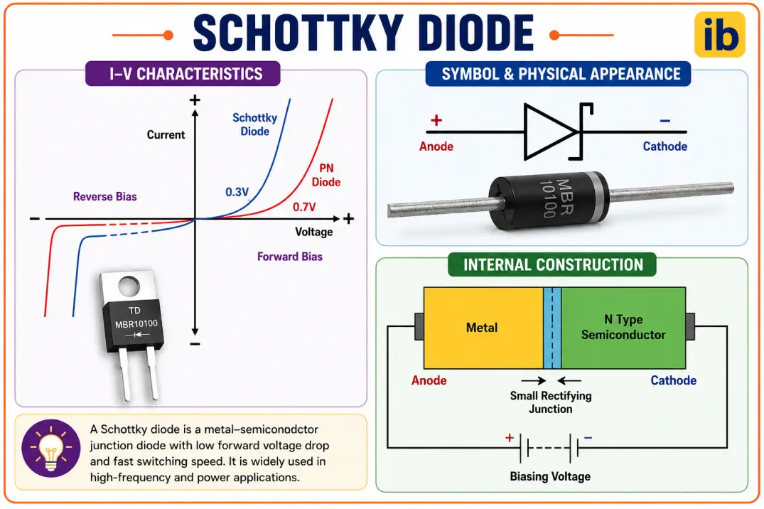
A Schottky diode is a metal-semiconductor junction diode with a low forward voltage drop and near-instant switching, made possible because it conducts using only majority carriers instead of the minority carrier process a standard PN junction relies on.
Named after physicist Walter Schottky, this diode skips the semiconductor-to-semiconductor junction entirely. A metal contact meets an N-type semiconductor directly.
That single structural change is responsible for nearly every advantage, and every limitation, this component is known for.
5 Proven Facts About the Schottky Diode
These five points explain the advantages, the tradeoffs, and the physics tying them together.
Metal-Semiconductor Junction, No True Depletion Region
A metal anode meets an N-type semiconductor cathode directly, forming a much thinner barrier than a PN junction's depletion zone.
Low Forward Voltage Drop
Typically 0.15 to 0.45 volts, compared to 0.6 to 0.7 volts for a standard silicon PN junction diode.
Near-Zero Reverse Recovery Time
Conduction relies only on majority carrier electrons, so there's no minority carrier storage to clear out when switching off.
Higher Reverse Leakage and Lower Breakdown Voltage
The same thin, low barrier that helps forward conduction also lets more current leak through in reverse, and limits how much reverse voltage it can block.
Conducts by Thermionic Emission
Electrons are emitted directly over the barrier by thermal energy, a fundamentally different mechanism than PN junction diffusion current.
Schottky Diode vs Standard PN Junction Diode
The construction difference cascades into every meaningful electrical difference between the two.
Schottky Diode
Metal-semiconductor junction. Low Vf, fast switching, higher leakage, lower reverse voltage rating.
PN Junction Diode
Semiconductor-semiconductor junction. Higher Vf, slower switching, lower leakage, higher reverse voltage rating.
Why the Same Barrier Creates Both the Advantage and the Limitation
It's tempting to think of the advantages and limitations as separate design choices. They're actually the same tradeoff viewed from two directions.
You cannot lower a Schottky diode's forward voltage without also raising its reverse leakage, since both come from the exact same barrier height. Choosing a Schottky diode always means choosing a specific point on that tradeoff curve.
Conduction Mechanism and Power Loss
Understanding forward conduction helps explain why Schottky diodes save real energy in switching circuits.
Simplified for engineers: lower φB directly lowers Vf, raising leakage current
Example: Vf = 0.4V (Schottky) vs 0.7V (PN), at I = 5A
Schottky: P = 0.4 x 5 = 2.0 W | PN junction: P = 0.7 x 5 = 3.5 W
Roughly 43% less forward conduction loss with the Schottky diode
Key Specifications: Schottky vs PN vs TVS/Zener
Choosing between clamping and rectifying technologies comes down to a handful of numbers.
| Parameter | Schottky Diode | PN Junction Diode |
|---|---|---|
| Forward voltage drop | 0.15 to 0.45 V | 0.6 to 0.7 V |
| Reverse recovery time | Near zero, nanoseconds | Tens to hundreds of nanoseconds |
| Typical max reverse voltage | Roughly 50 to 200V (silicon) | Up to several kV |
| Reverse leakage current | Higher, microamps to mA range | Lower, typically nanoamps |
Where Schottky Diodes Are Used
Switching Power Supplies
Output rectification where low Vf directly improves efficiency.
Solar Panel Blocking Diodes
Preventing battery discharge back through the panel at night.
RF Signal Detection
Fast response and low capacitance for envelope detection circuits.
TTL Logic Clamping
Preventing transistor saturation delay in classic Schottky TTL gates.
Sample-and-Hold Circuits
Fast, low-loss switching for precision analog circuits.
Automotive Reverse Battery Protection
Fast, efficient protection against wiring polarity mistakes.
Advantages and Limitations at a Glance
✓ Advantages
- Low forward voltage drop reduces conduction power loss
- Near-instant switching with essentially no reverse recovery time
- Low junction capacitance suits high-frequency applications
- Generates less switching noise than a comparable PN junction diode
✗ Limitations
- Higher reverse leakage current, especially as temperature rises
- Lower reverse breakdown voltage than typical PN junction rectifiers
- Higher unit cost compared to standard general-purpose diodes
- Leakage current worsens further at elevated operating temperatures
Live Schottky vs PN Junction Power Loss Calculator
Compare forward conduction power loss between a Schottky diode and a standard PN junction diode at the same current.
Why Reverse Leakage Gets Worse With Temperature
Thermionic emission is, by definition, a thermal process. That has a direct consequence for how these diodes behave as they heat up.
As junction temperature rises, more electrons gain enough thermal energy to cross the barrier in the reverse direction too, not just forward.
This is why Schottky diode datasheets show reverse leakage current climbing sharply at higher temperatures, and why thermal design matters more for Schottky rectifiers than for equivalent PN junction parts.
Reference Materials on Schottky Diodes
FAQs on Schottky Diodes
External References
- The Schottky Diode Tutorial, Electronics Tutorials
- Schottky Diode: Definition, Characteristics, Working, and Applications, Science Facts
- Schottky Diode Overview, Components101
- MBR1045 Schottky Diode Datasheet, Vishay
- Schottky Diode, Wikipedia
What we learn today
- A Schottky diode uses a metal-semiconductor junction instead of a PN junction, conducting through majority carrier electrons only.
- Its low forward voltage drop, typically 0.15 to 0.45V, reduces conduction power loss significantly compared to standard silicon diodes.
- Near-zero reverse recovery time comes from having no minority carrier storage to clear when switching off.
- The same low barrier height that lowers forward voltage also raises reverse leakage current and limits reverse breakdown voltage.
- Applications span switching power supplies, RF detection, solar panel protection, and historically, TTL logic gate clamping.