
A photodiode gives a tiny current, often only nanoamps or microamps, that no voltmeter or ADC can read directly. One op amp and one resistor turn that current into a clean, usable voltage when the circuit is designed carefully.
Light sensors, fibre receivers and pulse oximeters all depend on converting a weak photocurrent into a voltage. The transimpedance amplifier does this with high gain, low noise and a stable response.
What Is a Transimpedance Amplifier?
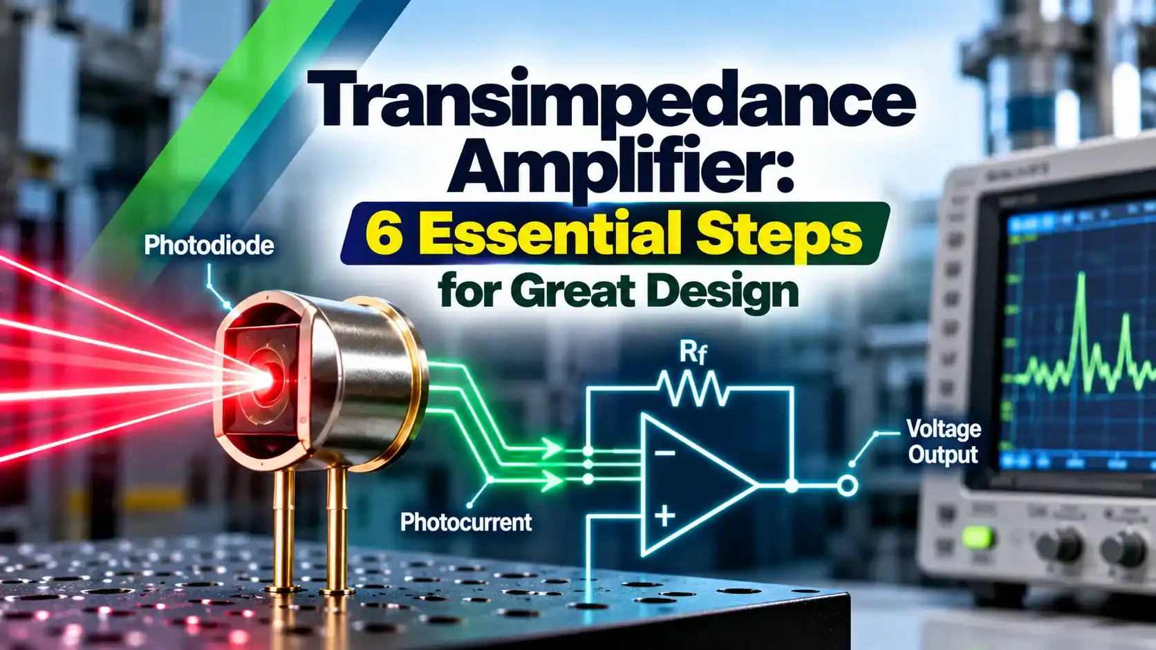
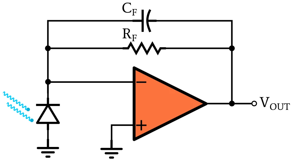
A transimpedance amplifier is an op amp circuit that converts an input current into a proportional output voltage, with gain expressed in ohms. The photodiode connects to the inverting input and a feedback resistor Rf sets the gain, using the principles covered in op amp basics.
Because negative feedback holds the inverting input at virtual ground, the photodiode sees almost zero volts across it. All of its current flows through Rf, so the output voltage magnitude equals photocurrent times Rf.
A photodiode is preferred over a phototransistor when linearity and speed matter, as compared in photodiode vs phototransistor. Slow, cheap light sensing can use an LDR instead, but it is far less linear.
How the Current to Voltage Conversion Works
A simple resistor to ground would also make a voltage, but the diode voltage would then change with light, which makes the response nonlinear and slow. The transimpedance amplifier keeps the diode voltage fixed, so linearity and speed improve together.
The gain of a transimpedance amplifier is measured in ohms, which is why it is called transimpedance or transresistance gain. A 1 MΩ feedback resistor gives 1 volt of output for every microamp of photocurrent.
Transimpedance Amplifier Gain, Bandwidth and Cf Formulas
Bandwidth: f3dB ≈ √(GBW ÷ (2π × Rf × Cin))
Feedback capacitor: Cf ≈ √(Cin ÷ (2π × Rf × GBW))
Cin = photodiode capacitance plus op amp input capacitance
Example:
Iph = 10 µA, Rf = 100 kΩ, GBW = 10 MHz, Cin = 20 pF
Vout = 10 µA × 100 kΩ = 1.000 V
f3dB = √(10 MHz ÷ (2π × 100 kΩ × 20 pF)) ≈ 892.1 kHz
Cf = √(20 pF ÷ (2π × 100 kΩ × 10 MHz)) ≈ 1.78 pF
The Cf rule places the feedback pole near the frequency where the noise gain meets the op amp open loop gain, giving about 45 degrees of phase margin. With that Cf, the closed loop corner 1 ÷ (2π × Rf × Cf) equals the same 892 kHz, so both formulas agree.
Phase margin and the loop gain crossing are easier to picture on a Bode plot, as explained in Bode plot gain and phase margin. A larger Cin always lowers the achievable bandwidth for a given Rf and op amp.
TIA Output and Bandwidth Calculator
The result is a first estimate for a transimpedance amplifier built on a single pole op amp and ignores parasitic capacitance across Rf. Choose the next standard capacitor value and confirm the step response in simulation or on the bench.
Second Worked Example: TI Photodiode Design
Texas Instruments describes a single supply design in its Analog Engineer circuit note SBOA220, using the OPA323 for 0 to 2.4 µA of photocurrent and 20 kHz bandwidth. With Rf = 2 MΩ, full scale output is 2.4 µA × 2 MΩ = 4.8 V.
The note limits the feedback capacitor to Cf ≤ 1 ÷ (2π × Rf × fp), which gives 3.98 pF for 20 kHz, and selects 3.3 pF. That value sets the corner at 1 ÷ (2π × 2 MΩ × 3.3 pF) ≈ 24.1 kHz, safely above the goal.
TI also adds a small offset so that the transimpedance amplifier output starts at 100 mV instead of zero. This keeps the single supply op amp away from its lower rail, where it cannot swing cleanly.
Photovoltaic vs Photoconductive Mode
| Feature | Photovoltaic, Zero Bias | Photoconductive, Reverse Bias |
|---|---|---|
| Diode voltage | About 0 V | Reverse voltage, for example 5 V |
| Dark current | Very low | Higher, rises with bias and heat |
| Junction capacitance | Highest | Lower, so faster |
| Noise | Lowest at low frequency | Extra shot noise from dark current |
| Best use | Precision, slow light meters | Fast receivers, lidar, pulses |
In photovoltaic mode the diode sits at virtual ground with no bias, which gives the lowest dark current and the best precision. In photoconductive mode a reverse bias widens the depletion layer, cutting capacitance and raising speed.
The choice is a trade between noise and speed, and the whole transimpedance amplifier design follows from it. For very small signals, the output is often followed by a Sallen and Key active filter to limit noise bandwidth.
Why the Transimpedance Amplifier Needs Cf
Analog Devices explains that the inverting feedback already contributes 180 degrees of phase shift, while the op amp dominant pole and the Rf with Cin network can each add about 90 degrees more. If the total reaches 360 degrees at unity loop gain, the circuit oscillates.
Cf adds a zero in the noise gain that cancels part of this phase lag. Analog Devices also advises designing with about 60 percent of the rated GBW, because process variation can shift it by around 40 percent.
If the output rings or oscillates on the bench, first try a slightly larger Cf. A small increase restores phase margin at the cost of a little bandwidth.
6 Essential Transimpedance Amplifier Design Steps
Steps two to five often loop a few times, since a bigger Rf improves noise but reduces bandwidth. The same feedback thinking appears in the op amp integrator and differentiator, where a capacitor shapes the response.
Transimpedance Amplifier Noise Explained
Eikonal Optics notes that shot noise from the photocurrent and dark current sets the fundamental limit on signal to noise ratio. It also shows that the Johnson noise of the feedback resistor often dominates at lower frequencies.
Signal grows in proportion to Rf, while the resistor current noise falls as 1 ÷ √Rf, so a larger Rf improves signal to noise ratio. You can check the result in decibels with the SNR calculator and the decibel guide.
At high frequency, op amp voltage noise is multiplied by the noise gain 1 plus Cin ÷ Cf, so a large photodiode capacitance creates a noise peak. Smaller diodes, reverse bias or bootstrapping reduce Cin and this peak.
A 1 GΩ feedback resistor is common in very low light instruments, giving 1 volt per nanoamp. Such circuits need op amps with femtoamp level input bias current.
Choosing the Op Amp for a Transimpedance Amplifier
- Input bias current far below the smallest photocurrent.
- Low input capacitance, since it adds to Cin.
- GBW high enough for the target bandwidth with margin.
- Low voltage noise density at the frequencies of interest.
- Output swing close to the rails on single supply.
- Low offset voltage, which appears across the photodiode.
FET or CMOS input op amps are usual because bipolar input bias current would swamp small photocurrents. If a differential or bridge signal must be read instead, see the instrumentation amplifier and the differential amplifier and CMRR.
- Linear output over many decades of light.
- Fixed diode voltage gives fast response.
- Gain set by a single resistor.
- Low noise with a suitable op amp.
- Needs careful Cf selection for stability.
- Bandwidth falls as Rf and Cin rise.
- Very high Rf is sensitive to leakage and humidity.
- Op amp input current adds error.
Transimpedance Amplifier Applications
Industrial ranging systems described in 3D lidar sensors rely on fast, low noise receivers of this type. The output often feeds a voltage follower buffer or an ADC driver.
Guard the transimpedance amplifier input trace with a ring driven at the same potential, and keep Rf close to the op amp. Surface leakage can easily exceed a few nanoamps on a humid board.
Layout and Troubleshooting Tips
Keep the photodiode close to the op amp, because every centimetre of trace adds capacitance and picks up interference. Shield the input in a metal can when working below the nanoamp range.
If the output clips at a rail with no light, check the diode polarity and the op amp offset. For signals that must be rectified or averaged later, the precision rectifier is a useful next stage, and instrumentation amplifier vs op amp helps when choosing parts.
TI Photodiode Amplifier Circuit PDF
Building a Photodiode Amplifier Video
Transimpedance Amplifier FAQ
It converts a small input current into a proportional output voltage using an op amp and a feedback resistor. The gain is expressed in ohms, so 1 MΩ gives 1 volt per microamp.
It is the standard front end for photodiodes and other current output sensors. The virtual ground input keeps the sensor voltage constant for good linearity.
Photodiode and op amp input capacitance form a pole with Rf that adds phase lag inside the loop. Without compensation, the circuit usually rings or oscillates at high frequency.
A small Cf across Rf adds a zero that restores phase margin. The rule Cf ≈ √(Cin ÷ (2π Rf GBW)) gives about 45 degrees of margin.
Use f3dB ≈ √(GBW ÷ (2π × Rf × Cin)) as a first estimate for a transimpedance amplifier with a single pole op amp. With 10 MHz GBW, 100 kΩ and 20 pF of input capacitance, it gives about 892 kHz.
A larger Rf or a larger input capacitance lowers this bandwidth quickly. A faster op amp or a smaller photodiode with less capacitance raises it again.
Photovoltaic mode uses zero bias across the diode, which gives the lowest dark current and the best precision. It suits slow light meters, colour sensors and analytical instruments.
Photoconductive mode adds reverse bias to reduce junction capacitance and increase speed. It is preferred for optical receivers and lidar, where the extra dark current noise is an acceptable price.
Choose Rf so the maximum photocurrent produces nearly full output swing without clipping. For example, 2.4 µA into 2 MΩ gives 4.8 V in the TI design note.
A larger Rf improves signal to noise ratio because the signal grows faster than the resistor noise. However, it also reduces bandwidth and makes the circuit more sensitive to board leakage.
Pick a FET or CMOS input op amp with very low input bias current and low input capacitance. Its GBW must support the target bandwidth of the transimpedance amplifier with some margin.
Also check voltage noise density and rail to rail output on single supply designs. Analog Devices advises planning with about 60 percent of the rated GBW to cover process variation.
They are used in fibre optic receivers, lidar, pulse oximeters, smoke and particle sensors, and laboratory spectrometers. Barcode scanners, light curtains and optical encoders use them too.
Any sensor that produces a current proportional to light or radiation can use this circuit. Only the Rf value, the capacitance and the bandwidth target change between these designs.
Related Articles
- Operational Amplifier Basics
- Photodiode vs Phototransistor Key Differences
- Bode Plot Gain and Phase Margin
- Signal to Noise Ratio Calculator
- Instrumentation Amplifier Working
External References
- Photodiode Amplifier Circuit SBOA220, Texas Instruments
- Stabilize Your Transimpedance Amplifier, Analog Devices
- Transimpedance Amplifier, Wikipedia
What We Learn Today
- A transimpedance amplifier holds the photodiode at virtual ground and gives an output voltage equal to photocurrent times the feedback resistor Rf.
- The feedback capacitor Cf ≈ √(Cin ÷ (2π Rf GBW)) prevents ringing, and bandwidth is roughly √(GBW ÷ (2π Rf Cin)).
- Photovoltaic mode gives the lowest noise for precision work, while reverse biased photoconductive mode lowers capacitance for fast receivers and lidar.