
Two traces that carry equal and opposite signals can shrug off noise and radiate very little, but only when they are routed as a true matched pair. A few layout rules for impedance, spacing, length and vias decide whether a fast link works first time.
USB, Ethernet, HDMI and LVDS all send data on two traces instead of one. Good differential pair routing keeps those two traces balanced so the receiver sees a clean difference signal and the noise cancels out.

What Is Differential Pair Routing?
Differential pair routing is the PCB layout practice of running two traces that carry complementary signals side by side, with controlled impedance, equal length and constant spacing, so the receiver reads only the voltage difference between them. It is a core topic in signal integrity for high speed PCB design and applies to nearly every modern serial interface.
The receiver is basically a differential amplifier with high CMRR. Noise that couples equally onto both traces appears as common mode voltage and is rejected, while the wanted signal appears as the difference and is amplified.
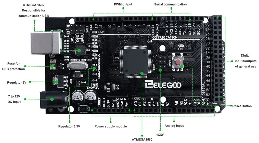
Altium uses this Arduino Mega board to show a practical rule: place the USB controller close to its connector so the pair stays short. A short route leaves fewer places for skew, crosstalk and impedance breaks to creep in.
Why Two Traces Beat One
A single ended signal uses the ground plane as its return, so any ground noise or ground bounce adds straight to the signal. A differential link carries its own return on the partner trace, which is why it tolerates lower voltage swings and faster edges.
The opposite currents also produce opposite magnetic fields that largely cancel at a distance, so a well balanced pair radiates less electromagnetic interference. The same principle is used in cables, as explained in shielded cable and twisted pair.
LVDS, defined in the TIA/EIA 644 standard, swings only about 350 mV across a 100 Ω termination. Such a small swing works only because the receiver looks at the difference, not at the voltage to ground.
Impedance Targets for Common Interfaces
| Interface | Differential Impedance | Typical Skew Rule | Notes |
|---|---|---|---|
| USB 2.0 | 90 Ω, TI window 81 to 99 Ω | 50 mils within pair | Up to 4 vias per trace per TI |
| USB 3.x, PCIe | 90 Ω USB 3, about 85 Ω PCIe | 5 mils within pair | USB 3 limited to 2 vias |
| HDMI TMDS | 100 Ω, TI window 90 to 110 Ω | 5 mils within pair | No vias preferred |
| Ethernet 100 and 1000BASE T | 100 Ω | Tight within pair | Short run to magnetics |
| LVDS | 100 Ω | Tight within pair | Terminate at receiver |
| CAN and RS 485 | About 120 Ω | Relaxed | Low speed, long cables |
The differential impedance depends on trace width, the gap between the two traces, dielectric height and material. Setting these values is explained in controlled impedance PCB traces, and your fabricator will tune the final geometry for its own stackup.
Slower buses such as CAN and RS 485 are differential too, but their long cables matter more than the board. The termination side of those networks is covered in RS 485 termination and biasing resistors.
Ask the PCB fabricator for an impedance controlled stackup before you start differential pair routing. Their calculated width and gap, based on the real prepreg and copper, is more accurate than any generic online calculator.
7 Smart Differential Pair Routing Rules
Texas Instruments recommends in its high speed layout guide that the space between one pair and any other signal is at least 5 times the trace width. It also asks for a 30 mil keep out from other signals and 50 mils from periodic or clock lines.
Changing the gap is the most common mistake, because every change in spacing changes the impedance and converts some differential signal into common mode noise. General layout advice in essential PCB design rules also applies, but the pair rules take priority on high speed nets.
Length Matching in Differential Pair Routing
Skew is the difference in arrival time of the two halves of the pair. If one trace is longer, its edge arrives late, the difference signal gets a slow step in the middle, and part of the energy turns into common mode noise that radiates.
Signals on FR4 travel at roughly 140 to 180 ps per inch depending on the effective dielectric constant. The delay per inch equals 84.7 ps multiplied by the square root of the effective dielectric constant, which is the basis of the calculator below.
Skew = Length mismatch in inches × Delay per inch
Unit interval UI = 1000 ÷ Data rate in Gbps ps
Example:
Mismatch = 50 mils = 0.05 inch, Dk effective = 3.4, data rate = 5 Gbps
Delay = 84.7 × 1.844 = 156.2 ps per inch
Skew = 0.05 × 156.2 = 7.81 ps
UI = 1000 ÷ 5 = 200.0 ps
Skew as share of UI = 7.81 ÷ 200 = 3.9 percent
Match length close to where the mismatch occurs, usually near the bend or the pin that caused it, using small serpentine bumps on the shorter trace. Keep the bump height below about twice the pair gap so the coupling does not change too much.
Differential Skew Calculator
Second Worked Example: USB 2.0 High Speed
Altium explains that USB 2.0 High Speed allows a maximum intra pair skew of 100 ps, with rise times of at least 500 ps. At about 156 ps per inch, 100 ps corresponds to roughly 0.64 inch, and Altium quotes a round figure of 0.6 inch.
Altium also gives an example coplanar geometry for 90 Ω on a two layer board, with 9.5 mil traces, a 5 mil gap and 5 mil spacing to ground. That shows USB 2.0 is forgiving, although TI still asks for 50 mils or less of skew as a safe design target.
Spacing and Coupling Choices
Gap about equal to trace width; strong field sharing between the two traces.
Gap two or more times the width; each trace behaves more like single ended.
Pair buried between two planes on an inner layer.
Eric Bogatin points out that the coupling within the pair matters less than many people think, because most of the return current still flows in the nearby plane. What matters most is a constant geometry, which is why a solid reference from ground plane PCB design is so important.
Coupling to other nets is a bigger risk, so keep pairs apart and avoid long parallel runs with aggressors. The methods described in PCB crosstalk reduction apply fully to differential pair routing.
Via Transitions During Differential Pair Routing
Every via is an impedance discontinuity and a possible stub. Use a symmetric pair of vias for the two traces, and choose the right via style from through hole, blind and buried vias for your layer count.
TI limits USB 3 pairs to two vias in total and asks designers to keep via stubs below about 15 mils, using back drilling on thick boards. Place a ground via next to each signal via so the return current can change planes with the signal.
When the pair moves between layers, check that both reference planes are ground, or stitch them with a capacitor if one is power. The layer order that makes this easy is covered in PCB layer stackup design.
TI guidance allows no stubs and no test points on high speed differential pairs. If you need probing, add test pads in line with the traces instead of branching off them.
Step by Step Layout Workflow
In differential pair routing, protection parts such as a TVS diode should sit right at the connector with the pair passing straight through their pads. Pick low capacitance parts, since a few picofarads can upset the impedance of a fast link.
Do differential pair routing first, before the general signals, while the board still has clean space. Fixing a pair later usually forces extra vias and bends that eat the skew budget.
- Strong rejection of common mode noise.
- Lower EMI from cancelling fields.
- Supports low voltage swing and high data rates.
- Predictable impedance and fewer reflections.
- Needs impedance controlled fabrication.
- Uses more routing space than single traces.
- Length tuning adds design time.
- Vias and connectors still break symmetry.
Where Differential Pairs Are Used
On industrial boards the CAN bus transceiver pair is slow enough that tight skew rules do not apply, yet a matched route still helps EMC. For Ethernet ports, keep the pair short to the magnetics, since the cable itself follows the limits in Ethernet cable length and types.
Troubleshooting Checklist
- Confirm the fabricator impedance report matches the target.
- Check that no split or slot sits under the pair.
- Review the length report for intra pair skew.
- Count vias and confirm ground vias sit beside them.
- Verify 5W spacing to neighbouring nets.
- Check ESD and common mode choke footprints for symmetry.
- Measure eye diagrams or TDR on a prototype when possible.
Most differential pair routing failures come from a plane split, a missing return via or a connector breakout that changes the gap. A time domain reflectometer quickly shows where the impedance jumps, as described in what is signal integrity.
TI High Speed Interface Layout Guidelines
Do Differential Pairs Need Ground? Video
Differential Pair Routing FAQ
It is the layout method of running two complementary signal traces together with controlled impedance, equal length and constant spacing. The receiver then reads only the voltage difference between the two traces.
Noise that reaches both traces equally is rejected as common mode. The result is a fast and robust link that also radiates very little noise.
USB designs target about 90 ohms differential, while Ethernet, LVDS and HDMI usually target 100 ohms. CAN and RS 485 networks work near 120 ohms, although their long cables matter more than the board layout.
The exact width and gap depend on the stackup and material. Ask your fabricator to calculate them and to test impedance coupons on the panel.
It depends on the data rate and the rise time of the interface in use. TI suggests 50 mils within a USB 2.0 pair and 5 mils for USB 3, PCIe, SATA and HDMI pairs.
Convert the mismatch into picoseconds using about 150 to 160 ps per inch on FR4. Keep that skew a small share of the unit interval.
Yes, in practice they almost always do on a printed circuit board. Much of the return current still flows in the nearest plane under the traces.
A split or slot under the pair forces that current to detour and creates common mode noise. Good differential pair routing runs over solid ground and stitches planes with vias at every layer change.
TI limits USB 3 pairs to two vias and USB 2.0 traces to four per trace. PCIe, SATA and HDMI pairs are best routed with no vias at all.
When vias are unavoidable, place them symmetrically for both traces. Add a ground via next to each one and keep every via stub as short as the board allows.
Tight coupling uses a gap close to the trace width, so the two traces share much of their field. Loose coupling uses a wider gap, and each trace behaves more like a single ended line.
Both can work well in real designs. The key rule in differential pair routing is to keep the chosen gap constant along the whole length.
Add serpentine tuning close to the point that created the mismatch, usually at a bend or at a connector pin. That keeps the two halves balanced for most of the route.
Keep each bump low and gentle so coupling does not change much. Avoid tuning inside the connector breakout where space and symmetry are already tight.
Related Articles
- Controlled Impedance PCB Traces
- Signal Integrity in High Speed PCB Design
- PCB Crosstalk Reduction
- PCB Layer Stackup Design
- Ground Plane PCB Design
External References
- High Speed Interface Layout Guidelines, Texas Instruments
- Routing Requirements for a USB Interface on a 2 Layer PCB, Altium
- Differential Signalling, Wikipedia
What We Learn Today
- Differential pair routing keeps two complementary traces at constant spacing and controlled impedance, usually 90 Ω for USB and 100 Ω for Ethernet and LVDS.
- Length mismatch becomes skew at roughly 150 to 160 ps per inch on FR4, so fast links need tight matching near the source of mismatch.
- Solid ground planes, few symmetric vias with nearby ground vias, and 5W spacing to other nets keep the pair balanced and quiet.