
A 3.3 V sensor wired straight to a 5 V board can be damaged, while a 3.3 V output may not look high enough to a 5 V input. The right translation method protects both sides and keeps every bit readable.
Mixed voltage boards are now normal, with 3.3 V microcontrollers talking to 5 V displays, relays and sensors. A logic level shifter chosen for the bus type and speed keeps both sides safe and every bit valid.
What Is a Logic Level Shifter?
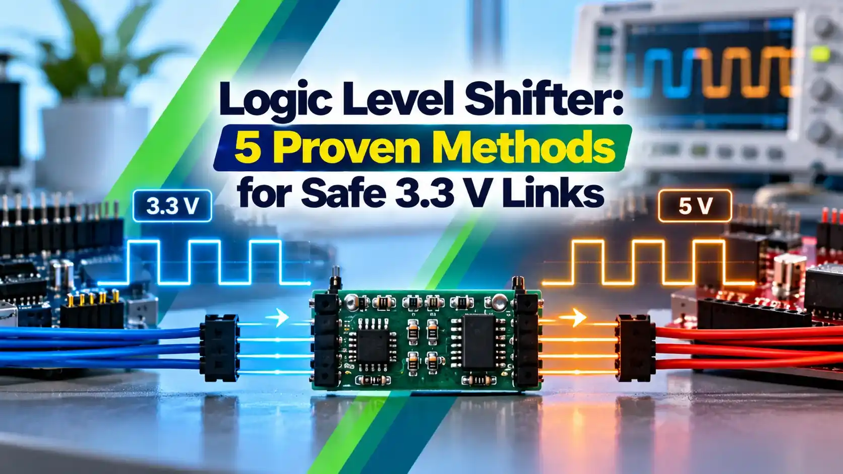
A logic level shifter is a circuit that translates digital signals between two supply voltages, such as 3.3 V and 5 V, so that a high on one side is read as a valid high on the other without overstressing any pin. It is needed whenever a modern microcontroller talks to an older 5 V module.
The problem has two halves. A 5 V output driving a 3.3 V input pushes current through the input protection diodes, and a 3.3 V output driving a 5 V input may sit below the high threshold described in TTL vs CMOS logic families.
A logic level shifter can be one way, such as a sensor output feeding a controller, or two way, such as an I2C data line shared by many devices.
Philips, now NXP, published the two resistor, one MOSFET bidirectional shifter for I2C in application note AN97055. The same circuit is still on most low cost blue level shifter boards sold today.
Understanding VIH, VIL and Noise Margins
Every logic input has a minimum voltage it accepts as high, called VIH, and a maximum voltage it accepts as low, called VIL. Every output has a guaranteed high, VOH, and a guaranteed low, VOL, at a stated load current.
| Family at Supply | VIH min | VIL max | Notes |
|---|---|---|---|
| 5 V TTL and 74HCT | 2.0 V | 0.8 V | Accepts 3.3 V outputs directly |
| 5 V CMOS 74HC | 3.5 V | 1.5 V | 0.7 and 0.3 of VCC, rejects 3.3 V |
| ATmega328P at 5 V | 3.0 V | 1.5 V | 0.6 and 0.3 of VCC, thin margin |
| 3.3 V LVCMOS | 2.0 V | 0.8 V | Usually not 5 V tolerant |
This table explains the most common surprise. A 3.3 V output easily satisfies a 74HCT or TTL input at 2.0 V, but a 74HC gate at 5 V needs 3.5 V and may read the same signal as undefined, a zone explained in digital logic gates.
Before buying any converter, check the receiver datasheet for VIH and the absolute maximum input voltage. Many 3.3 V to 5 V links need no translator at all, only a 74HCT buffer or a 5 V tolerant input.
5 Proven Logic Level Shifter Methods
Two resistors scale a 5 V output down to about 3.3 V.
One N channel MOSFET and two pull ups per line, as in NXP AN97055.
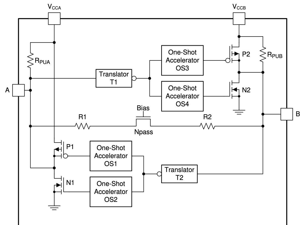
Pass transistor with one shot edge accelerators and internal pull ups.
Active buffers with weak 4 kΩ series resistors and edge detection.
74LVC245 or 74HCT family gates with a fixed or controlled direction.
A voltage divider is fine for a 5 V output entering a 3.3 V input at modest speed.
The MOSFET circuit and the TXS family suit open drain buses, while the TXB family and dedicated buffers suit push pull links such as SPI and UART. Matching the logic level shifter to the bus is the main design rule.
How the BSS138 Logic Level Shifter Works on I2C
In the classic logic level shifter, the gate of an N channel MOSFET goes to the low supply, the source goes to the low side line with its own pull up, and the drain goes to the high side line with a pull up to 5 V. NXP AN97055 lists three states that make it bidirectional without any direction pin.
NXP states that the gate threshold should be between 0.1 V and 2 V, and that the circuit works down to about 2 V on the lower side and up to 10 V or more on the higher side. The BSS138 has a typical threshold near 1.3 V, which suits a 3.3 V gate drive.
Because rising edges come only from the pull up resistors, the speed of this logic level shifter is set by resistor value and bus capacitance. It is ideal for 100 kHz and 400 kHz I2C, as compared in SPI vs I2C, but weak for fast SPI clocks.
In the MOSFET shifter, the low supply must stay at or below the high supply. If the 3.3 V rail powers up after the 5 V rail, the bus can see odd levels for a moment, so power sequencing still matters.
Divider Formula and Margin Check
VIH = 0.7 × VDD of receiver
Margin = Vout minus VIH
Example:
Vin = 5 V, R1 = 1 kΩ, R2 = 2 kΩ, VDD = 3.3 V
Vout = 5 × 2 ÷ 3 = 3.33 V
VIH = 0.7 × 3.3 = 2.31 V
Margin = 3.33 minus 2.31 = 1.02 V, safe
Vout must also stay below the receiver absolute maximum, usually VDD plus 0.3 V. Here 3.33 V is below 3.6 V, so the input is protected.
Voltage Divider Level Shift Calculator
Second Worked Example: Divider Speed Limit
Suppose you use 10 kΩ and 20 kΩ to save current, and the receiving pin plus wiring adds 10 pF. The source sees the two resistors in parallel, 6.67 kΩ, so the time constant is 6.67 kΩ × 10 pF = 66.7 ns.
The 10 to 90 percent rise time is about 2.2 times that, or 147 ns, which is acceptable for a 115200 baud UART but rounds off a fast SPI clock badly. The same RC behaviour is explained in RC low pass filters.
TXS0108E vs TXB0108: Choosing the IC
Texas Instruments rates the TXS0108E for 1.4 V to 3.6 V on the A port and 1.65 V to 5.5 V on the B port, with VCCA never above VCCB. Its datasheet quotes 110 Mbps push pull and 1.2 Mbps open drain at 3.3 V to 5 V.
The TXS0108E has dynamic internal pull ups of 40 kΩ while a line is low and 4 kΩ while it is high, plus one shot circuits that speed up edges.
The TXB0108 uses active buffers behind roughly 4 kΩ series resistors and can reach 100 Mbps. TI states clearly that it should not be used where an open drain driver is connected, such as I2C or 1 Wire.
- Works with open drain I2C and MDIO lines.
- Internal pull ups save parts.
- OE pin gives clean power sequencing.
- B port ESD rated to 8 kV contact.
- Strong push pull edges up to 100 Mbps.
- No pull up current in steady state.
- Good for SPI, UART and parallel GPIO.
- Small footprint for eight lines.
Big Mess o Wires tested the TXS0108 and found that even a 6 inch wire could trigger oscillation, because its one shot of about 30 ns reacts to reflections. The same author found that the TXB0104 needs drivers able to supply at least 2 mA.
When a TXS0108E board misbehaves on jumper wires, shorten the wires, add a small series resistor of about 22 to 33 Ω near the driver, or move to a MOSFET shifter for slow lines.
Selecting the Right Translator
For a single 5 V HC SR04 ultrasonic sensor echo pin into a 3.3 V board, a divider is enough. For an I2C display shared by several 3.3 V and 5 V devices, the MOSFET logic level shifter is the safer and cheaper choice.
A 5 V signal into a 3.3 V pin may appear to work because current flows through the input clamp diode into the 3.3 V rail. That hidden current can raise the rail itself when the board draws little load.
Troubleshooting a Logic Level Shifter
- Confirm the low supply goes to LV and the high supply to HV.
- Measure both supplies and confirm VCCA is not above VCCB.
- Check that OE is pulled high on TXS and TXB boards.
- Look at rising edges on a scope for slow rounding or ringing.
- Count pull ups on I2C, since modules often add their own.
- Confirm a common ground between both boards.
- Remove external pull ups below 50 kΩ when using a TXB0108.
If an I2C scan finds nothing, swap SDA and SCL first, then measure the idle level on each side, which should sit at its own supply. A stuck low line usually means a device is holding the bus or a pull up is missing; compare this with how pull ups behave on RS485 biasing resistors.
For noisy industrial wiring where ground potential differs between panels, use a digital isolator or an optocoupler rather than a plain shifter. A plain logic level shifter has no isolation barrier at all.
Where a Logic Level Shifter Is Used
NXP AN97055 Bidirectional Level Shifter Note
Voltage Level Shifting Video Tutorial
Logic Level Shifter FAQ
It translates digital signals between two supply voltages, such as 3.3 volts and 5 volts. A high on one side then appears as a valid high on the other side.
It also protects lower voltage pins from damaging current. Without it, a 5 volt output can push current into a 3.3 volt input through its clamp diodes.
Sometimes yes, if the 5 volt input has a TTL style threshold of about 2 volts. Parts in the 74HCT family and many TTL compatible chips accept 3.3 volt highs easily.
A 74HC gate at 5 volts needs about 3.5 volts for a high, so it may fail. Always compare the driver output high with the receiver input high in the datasheets.
It is a small N channel MOSFET with a low gate threshold near 1.3 volts. A 3.3 volt gate supply therefore turns it fully on when either side pulls low.
Its body diode lets the 5 volt side pull the 3.3 volt side down first. That behaviour gives true bidirectional operation without any direction control pin.
Choose the TXS0108E for open drain buses such as I2C, because it has internal pull ups and one shot edge accelerators. It also handles mixed open drain and push pull lines.
Choose the TXB0108 for push pull links such as SPI and UART that need speed. Texas Instruments warns that the TXB0108 should not be used with open drain drivers.
A divider works well for one way signals from a 5 volt output into a 3.3 volt input. Values such as 1 kilohm and 2 kilohm give about 3.33 volts.
It cannot raise a 3.3 volt signal to 5 volts or work in both directions. Large resistor values also slow the edges because of input capacitance.
Its rising edges come only from the pull up resistors charging the bus capacitance. That makes it suitable for standard and fast mode I2C at 100 and 400 kilohertz.
For faster signals, lower the pull up values or move to a buffered translator. Always check the edge shape on an oscilloscope after making the change.
Yes, both boards must share the same ground reference for the voltage levels to mean anything. A missing ground often shows as random bits or no communication at all.
If the grounds cannot be joined safely, use a digital isolator or optocoupler instead. These devices pass the signal across an insulation barrier without a shared ground.
Related Articles
- SPI vs I2C Protocol Comparison
- TTL vs CMOS Logic Families
- What Is a MOSFET and How It Works
- Voltage Divider Rule Explained
- Schmitt Trigger Hysteresis
External References
- AN97055 Bi Directional Level Shifter for I2C Bus, Philips Semiconductors
- A Tale of Three Bidirectional Level Shifters, Big Mess o Wires
- Logic Level, Wikipedia
What We Learn Today
- A logic level shifter translates signals between supplies such as 3.3 V and 5 V while keeping VIH and VIL margins positive on both sides of the link.
- The BSS138 MOSFET circuit from NXP AN97055 gives true bidirectional translation for I2C, using only one transistor and two pull up resistors per line.
- Choose the TXS0108E for open drain buses and the TXB0108 for fast push pull SPI or UART, because TI warns the TXB0108 must not drive I2C.