
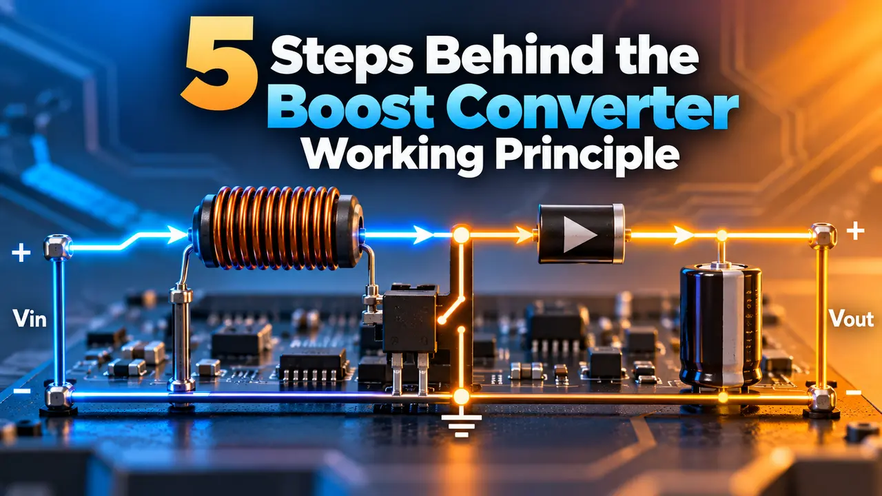
The Boost Converter Working Principle explains how a circuit takes a lower input voltage and produces a higher output voltage using nothing more than a switch, an inductor, a diode, and a capacitor.
The Boost Converter Working Principle relies on an inductor storing energy while a switch is closed, then releasing that energy into the output at a higher voltage once the switch opens.
This pairs naturally with Buck Converter Working Principle, since both circuits use the same basic switching building blocks to move voltage in opposite directions.
Boost Converter Working Principle
A boost converter is a switching regulator that produces an output voltage higher than its input, something a simple resistive circuit could never do without wasting most of the energy as heat.
It achieves this by rapidly switching an inductor between a charging state and a discharging state, using the inductor's own resistance to sudden current change to push voltage upward.
Four components do essentially all the work, a switch, an inductor, a diode, and an output capacitor, arranged so energy flows in one direction only once the switch opens.
Selecting the right diode also means understanding the different diode types available, since reverse recovery speed directly affects switching losses.
The ratio of switch on time to total switching period, called duty cycle, is what ultimately decides how much higher the output voltage climbs above the input.
Choosing the right switch matters just as much, and the MOSFET working principle explains why this device dominates modern switching regulator designs.
5 Steps in Every Switching Cycle
Key Components and Their Role
Stores and releases energy every switching cycle, the actual mechanism that pushes voltage above the input level.
Turns on and off at high frequency, controlled by the duty cycle that sets the output voltage.
Blocks reverse current when the switch is closed, only conducting when the inductor voltage spikes.
Smooths pulsed current from the diode into a steady output voltage the load can actually use.
Current Path Through the Circuit
While the switch is closed, the inductor charges from the source and the diode blocks any path to the output. The moment the switch opens, that stored energy pushes forward through the diode instead.
The Duty Cycle Formula
Example:
Input voltage = 5 V
Duty cycle = 0.6, meaning 60 percent on time
Output voltage = 5 divided by (1 minus 0.6)
Output voltage = 5 divided by 0.4 = 12.5 V
Boost vs Buck vs Buck Boost
| Converter Type | Voltage Relationship | Typical Use |
|---|---|---|
| Boost | Output always higher than input | Battery powered devices needing a higher rail |
| Buck | Output always lower than input | Stepping down a supply for logic circuits |
| Buck Boost | Output can be higher or lower than input | Wide input range battery applications |
Where Boost Converters Are Used
Common Mistakes When Designing a Boost Converter
Ignoring the right half plane zero: boost converters have a control characteristic that limits how fast the feedback loop can respond, and ignoring it leads to an unstable design.
Undersizing the inductor for peak current, and skipping proper diode selection for reverse recovery speed, are two more frequent errors that show up as excess heat or reduced efficiency.
Verifying a Boost Design on the Bench
Before trusting any calculated output figure, a designer should confirm the switching waveform on an oscilloscope. Probing the switch node shows whether the transistor is turning fully on and fully off.
A soft or ringing edge on that node usually points to a layout issue rather than a component fault, since long gate traces or a poorly placed decoupling capacitor can slow the switching transition enough to raise losses noticeably.
Thermal checks matter just as much as electrical ones. The inductor, the switch, and the diode all warm up during normal operation.
A quick check with a thermal camera after ten minutes at full load reveals whether any single part is running hotter than the rest.
An inductor that saturates before reaching its rated current will show a sudden jump in ripple current and a matching jump in temperature, which is a clear sign it needs to be replaced with a larger part.
Cost and size tradeoffs also shape real designs. Raising the switching frequency lets an engineer use a smaller inductor and capacitor, which saves board space and often lowers total cost, but it also raises switching losses.
Most practical designs settle somewhere between one hundred kilohertz and one megahertz, similar to the tradeoffs seen when comparing linear vs switching voltage regulators.
Input and output capacitor selection deserves the same attention as the inductor. Ceramic capacitors with low equivalent series resistance keep output ripple small and respond quickly to sudden load changes.
Electrolytic capacitors add bulk capacitance at a lower cost for applications where a bit more ripple is acceptable, so mixing both types on the output rail is a common and effective compromise.
Output Voltage Calculator
Reference Document
Watch: Boost Converter Explained
Boost Converter Working Principle FAQs
Related Articles on This Site
- Buck Converter Working Principle
- Linear vs Switching Voltage Regulators
- Voltage Regulator ICs Explained
- Inductor Working Principle
- MOSFET Working Principle
External References
What We Learn Today
- The Boost Converter Working Principle relies on an inductor storing and releasing energy every switching cycle.
- Duty cycle directly sets output voltage, following a simple, predictable formula.
- A boost converter can only step voltage up, never down, unlike a buck boost topology.