A freewheeling diode drops about half a volt on every off cycle, and at low output voltages that drop eats a big slice of the power. Replacing it with a MOSFET that switches in step with the main switch turns that wasted heat into useful output.
In a classic buck converter a Schottky diode carries the inductor current while the main switch is off. Synchronous rectification swaps that diode for a low resistance MOSFET, cutting loss and heat, as long as the timing is right.

What Is Synchronous Rectification?
Synchronous rectification is the use of an actively switched MOSFET in place of a rectifier diode, turned on exactly when the diode would conduct, so that current flows through a small channel resistance instead of a fixed junction drop. In a buck converter that MOSFET sits in the low side position, between the switch node and ground.
A diode always drops a near fixed voltage, while a MOSFET behaves like a resistor when fully on. The basics of that channel are explained in MOSFET working principle, and the low resistance is what makes the swap worthwhile.
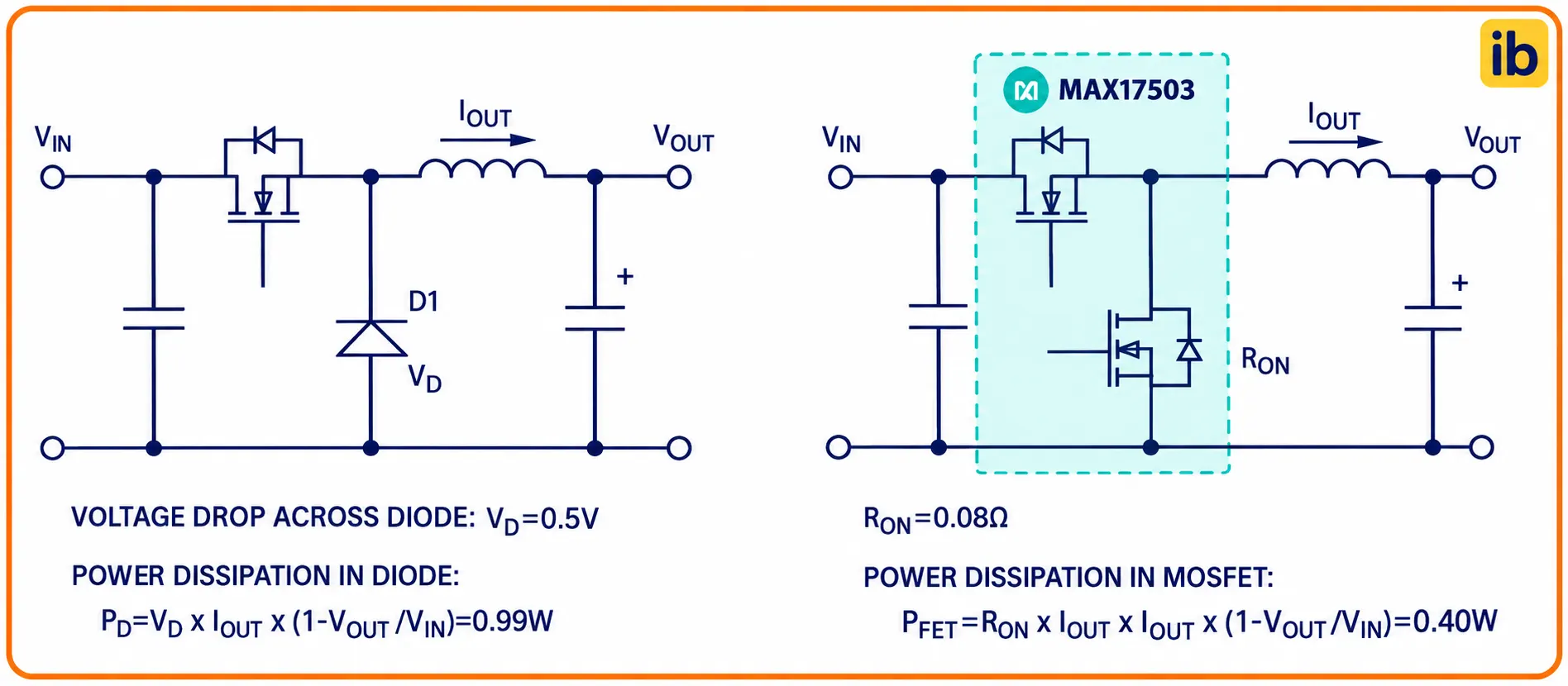
When a buck output is 3.3 V or lower and the load is more than about 1 A, check a synchronous part first. The saving at those levels is usually large enough to remove a heatsink.
Diode Versus MOSFET in the Freewheeling Path
In a non synchronous buck the freewheeling device is usually a Schottky diode, chosen for its low forward drop and fast recovery, as covered in Schottky diode advantages and limitations. Without synchronous rectification, that drop stays near 0.4 to 0.5 V at moderate currents and rises with load.
Analog Devices explains that at an output below 1 V, a diode drop of about 1 V means the converter works at roughly only 50 percent efficiency while the diode conducts. A MOSFET with a few milliohms of resistance drops only tens of millivolts at the same current.
In its 24 V to 5 V, 2.5 A example, Analog Devices reports that rectifier losses fall from 0.99 W with a diode to 0.4 W with synchronous rectification, more than halved. It adds that the converter temperature rise in that example is 30 °C.
| Point | Diode Rectification | Synchronous Rectification |
|---|---|---|
| Drop while conducting | Fixed, about 0.4 to 0.5 V Schottky | I × RDS(on), often tens of mV |
| Control needed | None | Gate drive and timing |
| Light load behaviour | Blocks reverse current | Can sink current unless diode emulation is used |
| Risk of shoot through | None | Yes, if timing fails |
| Cost and complexity | Lower | Higher |
| Best for | High output voltage, low current | Low voltage, high current rails |
How a Synchronous Buck Cycle Works
The controller produces two complementary signals from one PWM duty cycle. The high side is on for D = Vout ÷ Vin of each period, and the low side MOSFET covers the remaining 1 minus D.
The inductor current never stops during the off time, so something must carry it. With synchronous rectification that path is the MOSFET channel for most of the off time and its body diode only during the short dead times.
A power MOSFET can conduct from source to drain as well as drain to source when its gate is on. Synchronous rectifiers use exactly this reverse conduction, so current flows the same way as through the body diode but with far lower drop.
Conduction Loss Formula for Diode and MOSFET
ROHM gives the simplified low side loss of a synchronous buck as Iout squared times RDS(on) times 1 minus D, and the dead time loss as VD times Iout times the total dead time times the switching frequency. The diode version is simply the forward drop times Iout times 1 minus D.
MOSFET loss: P = Iout² × RDS(on) × (1 minus D) + Vbd × Iout × 2td × fsw
Example:
Vin = 12 V, Vout = 5 V, so D = 0.417 and 1 minus D = 0.583
Iout = 3 A, Vf = 0.5 V, RDS(on) = 70 mΩ
td = 30 ns per edge, fsw = 1 MHz, Vbd = 0.7 V
Diode: 0.5 × 3 × 0.583 = 0.875 W
MOSFET channel: 9 × 0.07 × 0.583 = 0.367 W
Dead time: 0.7 × 3 × 60 ns × 1 MHz = 0.126 W
Synchronous total = 0.493 W, saving 0.381 W
Synchronous Rectification Loss Calculator
Second Worked Example: A 1.2 V Core Rail
Take a 5 V to 1.2 V rail for a processor at 5 A, switching at 500 kHz. Here 1 minus D = 1 minus 0.24 = 0.76, so a 0.45 V Schottky loses 0.45 × 5 × 0.76 = 1.71 W, which is 28.5 percent of the 6 W output.
A 10 mΩ MOSFET loses 25 × 0.01 × 0.76 = 0.19 W in its channel. With 20 ns per edge and 0.7 V across the body diode, dead time adds 0.7 × 5 × 40 ns × 500 kHz = 0.07 W, so the total is only 0.26 W.
This is why low voltage point of load rails on processor and FPGA boards use synchronous rectification. A diode there would waste more power than many of the loads it feeds.
Dead Time in Synchronous Rectification
Dead time is the short gap when both MOSFETs are off, added so that one switch is fully off before the other turns on. During that gap the inductor forces current through the body diode of the low side MOSFET.
Analog Devices notes that this body diode has a relatively high forward drop and a long reverse recovery time, so a long dead time adds dissipation. When the high side turns on again, the stored charge of the body diode must be swept out, which adds a current spike and switching loss.
A Schottky in parallel with the low side MOSFET conducts before the body diode, which Analog Devices says improves performance at extra cost. The recovery spike also explains why a snubber circuit is sometimes added on the switch node.
Measure the switch node with a short ground spring on the probe, not the long ground lead. The long lead adds ringing that looks like a dead time fault but comes from the probe itself.
Shoot Through and How to Prevent It
In synchronous rectification, shoot through happens when the high side and low side MOSFETs are on together, even for a few nanoseconds. Input voltage is then shorted through both channels, causing a large current pulse, heating and, in the worst case, failed devices.
Controllers prevent it with adaptive dead time, which senses the gate or switch node voltage before turning the next MOSFET on. Gate driver details are covered in MOSFET gate driver ICs, and a strong pull down on the low side gate also prevents false turn on.
A fast rising switch node can couple through the drain to gate capacitance of the low side MOSFET and lift its gate above threshold. This effect, known as Cdv/dt turn on, can cause shoot through even when the controller timing is correct.
Synchronous Rectification at Light Load
A synchronous MOSFET can conduct in both directions, so at light load the inductor current can fall below zero and flow back from the output. Analog Devices describes this as continuous conduction with synchronous rectification, which keeps the frequency fixed but lowers light load efficiency.
Many controllers therefore offer a diode emulation or discontinuous mode, turning the low side off when its current reaches zero, and a pulse frequency mode at very light loads. These modes matter for battery powered designs where standby current sets runtime, as in battery backup time calculation.
Synchronous Rectification Controllers and MOSFETs
Both MOSFETs, driver and control in one IC.
Controller drives two external MOSFETs.
Several synchronous stages run out of phase.
6 Smart Steps to Design a Synchronous Rectification Stage
The hot loop layout matters as much as the parts, since loop inductance turns fast edges into ringing and EMI. Place the input decoupling capacitors right at the MOSFETs and use thermal vias under exposed pads.
- Gate signals never overlap at any load or temperature.
- Switch node ringing is within the MOSFET voltage rating.
- Body diode conduction time matches the intended dead time.
- Light load mode behaves as set, with no unwanted reverse current.
- MOSFET case temperature is within limits at full load.
- Efficiency is measured at light, half and full load.
- Much lower conduction loss at low output voltage.
- Cooler parts, often no heatsink needed.
- Fixed frequency possible down to zero load.
- Enables very high current point of load rails.
- Needs gate drive and accurate timing.
- Shoot through risk if timing fails.
- Can sink reverse current at light load.
- Higher cost and more complex layout.
Where Synchronous Rectification Is Used
The same idea appears in isolated supplies, where secondary MOSFETs replace the output diodes of a flyback converter. It is also used in boost converters, where the MOSFET replaces the output diode instead of a freewheeling one.
ROHM Buck Converter Efficiency Note
Video on Synchronous Rectification
Synchronous Rectification FAQ
It replaces a rectifier diode with a MOSFET that is switched on whenever the diode would conduct. Current then flows through the low channel resistance instead of a junction drop.
In a buck converter this MOSFET is the low side switch. It works in step with the high side switch, which is where the name comes from.
A Schottky diode drops roughly 0.4 to 0.5 V at moderate current, whatever the load voltage is. A MOSFET drops only the current times its on resistance, often tens of millivolts.
Analog Devices reports rectifier losses falling from 0.99 W to 0.4 W in a 24 V to 5 V, 2.5 A example. The gain grows as the output voltage falls.
Dead time is the short gap when both MOSFETs are off between transitions. It prevents both switches from conducting at once and shorting the input.
During the gap the body diode of the low side MOSFET carries the inductor current. Too long a gap wastes power, and too short a gap risks shoot through and failed MOSFETs.
Shoot through occurs when the high side and low side MOSFETs conduct at the same moment. Poor timing, slow turn off or Cdv/dt induced gate turn on can all cause it.
The result is a current spike, extra heat and possible device failure. Adaptive dead time and strong low side gate pull down are the usual cures.
Yes, because in synchronous rectification it conducts during every dead time interval. Its forward drop and reverse recovery charge both add loss, heat and switching noise.
Analog Devices notes that a Schottky diode placed in parallel can conduct before the body diode does. Some MOSFETs also include an integrated Schottky in the same package for this reason.
A diode suits high output voltages and low currents, where its drop is a small share of the output. It also needs no gate drive and cannot cause shoot through.
Simple auxiliary supplies and cost sensitive designs often keep the diode. Compare both losses with the calculator above before you decide on a topology for your rail.
The low side MOSFET can let inductor current reverse and flow back from the output capacitor. That keeps a fixed switching frequency but lowers efficiency at light load.
Many controllers use diode emulation to switch off the low side MOSFET at zero current. Pulse frequency mode then reduces switching losses further in battery powered products.
Related Articles
- Buck Converter Working Principle
- MOSFET Gate Driver ICs Explained
- Schottky Diode Advantages and Limitations
- MOSFET Working Principle
- Snubber Circuit RC Design
External References
- Efficiency of Buck Converter, ROHM Application Note
- How to Optimize Performance When Using Synchronous Rectification in Nonisolated DC to DC Converters, Analog Devices
- Active Rectification, Wikipedia
What We Learn Today
- Synchronous rectification replaces the freewheeling diode of a buck with a low side MOSFET, so the loss becomes current squared times RDS(on) instead of a fixed drop.
- Dead time keeps both MOSFETs off briefly to prevent shoot through, but the body diode conducts during that gap and adds loss.
- At low output voltages the saving is large, with 1.71 W of diode loss falling to about 0.26 W on a 1.2 V, 5 A rail.