
Two copper conductors at different voltages need enough distance through air and along the board surface to stop flashover and tracking. Getting creepage and clearance right is the first step toward a PCB that passes safety testing and protects its users.
Clearance protects a circuit board against short voltage transients through air, while creepage protects it against slow tracking along a dirty surface. Both depend on voltage, environment, board material and altitude.
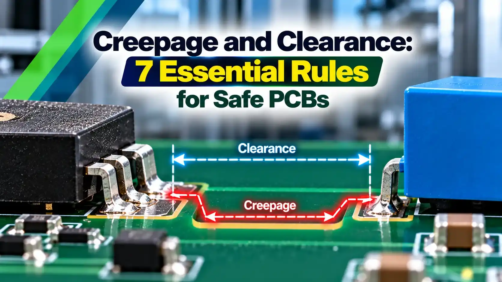
What Is Creepage and Clearance on a PCB?
Creepage and clearance are the two minimum insulation distances between conductors on a printed circuit board. Clearance is the shortest path through air, while creepage is the shortest path along the surface of the insulating material, as explained in our guide to electrical insulation.
Texas Instruments explains in its application note that creepage handles long term steady state working voltage, while clearance handles short term transients. It also notes that creepage can never be smaller than clearance, because the surface path can never be shorter than the straight air path.
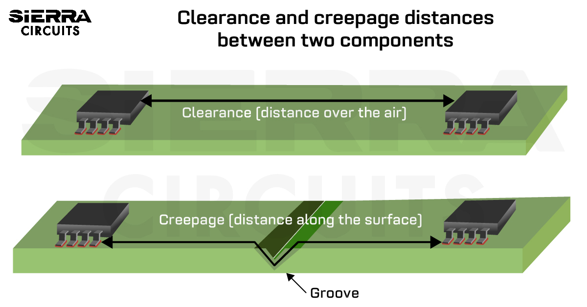
Sierra Circuits notes that these spacings become a product safety issue once the operating voltage rises above 30 V AC or 60 V DC. Below that level, spacing is usually set by manufacturing limits covered in essential PCB design rules.
Why Air and Surface Paths Fail Differently
Air breaks down within microseconds once the field ionises the gas. Therefore the peak transient voltage, not the average, decides the required clearance.
Surface failure is slower and is called tracking. Moisture and dirt form a conductive film, tiny arcs burn the resin, and a carbon track grows until the gap is bridged.
Air at 5000 m altitude is thin enough that the same gap flashes over at a noticeably lower voltage than at sea level. That is why IEC 60664 1 adds a correction factor of 1.48 at 5000 m for clearance.
Standards That Set Creepage and Clearance
IEC 60664 1 is the basic insulation coordination standard for low voltage equipment, and most product standards borrow its method. IEC 62368 1 covers IT and communication equipment, and IEC 61010 1 covers measurement and control equipment.
IPC 2221 is a generic PCB design standard with a single spacing table that lists voltage ranges against board location and coating. It is useful for functional spacing, but safety certification always follows the end product standard.
| Standard | Scope | Key Inputs |
|---|---|---|
| IEC 60664 1 | Basic insulation coordination | Impulse voltage, PD, CTI, altitude |
| IEC 62368 1 | IT, audio and ICT products | Working voltage, mains transients |
| IEC 61010 1 | Measurement and control equipment | Measurement category, PD |
| IPC 2221 | Generic PCB layout | Voltage range, location, coating |
Industrial transmitters and controllers usually fall under IEC 61010 1, while switch mode power supplies inside a 24 V PLC panel are usually certified to IEC 62368 1. Confirm the applicable standard with the test lab early.
Key Inputs: Pollution Degree, CTI and Overvoltage Category
Pollution degree describes how dirty and humid the micro environment around the board is. Texas Instruments lists four levels, from sealed equipment in degree 1 up to continuously wet outdoor conditions in degree 4.
No pollution or only dry pollution.
Dry pollution with occasional condensation.
Conductive pollution or frequent condensation.
Persistent conductivity from rain or snow.
Material group is based on the Comparative Tracking Index, the voltage at which a standard wet test creates a track on the laminate. Texas Instruments gives Group I as 600 V and above, Group II from 400 to 599 V, Group IIIa from 175 to 399 V and Group IIIb from 100 to 174 V.
Standard FR4 usually falls in Group IIIa unless the laminate datasheet proves a higher CTI. A higher CTI material allows smaller creepage, which is how isolation IC makers shrink packages.
Overvoltage category describes the transient level at the connection point, with plug in equipment in category II and fixed installations in category III. It sets the rated impulse voltage for clearance, as discussed in TVS diode protection.
If the laminate datasheet does not state a CTI value, treat the board as material Group IIIb in your calculation. It costs a little extra spacing but removes an argument with the test lab.
Worked Example: 230 V Mains Basic and Reinforced Isolation
Consider a 230 V AC mains board, category II, pollution degree 2, FR4 in group IIIa, below 2000 m. The creepage and clearance values below come from IEC 60664 1, with a rated impulse of 2.5 kV for basic insulation.
Basic insulation (live to earthed metal):
Clearance for 2.5 kV impulse = 1.5 mm
Creepage for 250 V rms working = 2.5 mm
Reinforced insulation (mains to SELV user side):
Impulse raised one step to 4 kV
Clearance = 3.0 mm
Creepage = 2 × 2.5 mm = 5.0 mm
Reinforced insulation doubles the creepage value and uses the next higher impulse voltage for clearance. Many designers add margin for board tolerances.
The same rule governs the gap under an optocoupler or isolation transformer. The package itself must offer enough creepage between its pins, and the PCB footprint must not reduce it with wide pads.
Second Worked Example: 48 V Telecom Board
A 48 V DC board sits below the 60 V DC safety threshold, so IPC 2221 guides its functional spacing. Sierra Circuits quotes the IPC 2221B value of 0.6 mm for uncoated external conductors carrying 31 to 50 V below 3050 m.
Internal layers need far less, because the laminate itself is the insulation and no surface contamination can reach it.
| Voltage Range | B1 Internal | B2 External Uncoated | B4 External Coated |
|---|---|---|---|
| 16 to 30 V | 0.05 mm | 0.1 mm | 0.05 mm |
| 31 to 50 V | 0.1 mm | 0.6 mm | 0.13 mm |
| 151 to 300 V | 0.2 mm | 1.25 mm | 0.4 mm |
Altitude Correction for Clearance
Clearance tables in IEC 60664 1 assume an altitude up to 2000 m. Above that, the standard gives multiplication factors, and Texas Instruments shows an example where a 3.6 mm clearance becomes 5.33 mm at 5000 m using the factor 1.48.
| Altitude | Multiplication Factor |
|---|---|
| 2000 m | 1.00 |
| 3000 m | 1.14 |
| 4000 m | 1.29 |
| 5000 m | 1.48 |
| 6000 m | 1.70 |
Many Indian hydro and telecom sites sit above 2000 m, so creepage and clearance checks there must include this factor. Creepage itself needs no correction, because tracking depends on surface film, not air density.
Creepage and Clearance Margin Calculator
This calculator applies the IEC 60664 1 altitude factor to a clearance value you read from the correct table, then compares it with your layout spacing. It interpolates linearly between table points from 2000 m to 10000 m, which is a common engineering practice.
Margin % = (Actual minus Corrected) ÷ Corrected × 100
Example:
Reinforced clearance 3.0 mm at 3000 m
Corrected = 3.0 × 1.14 = 3.42 mm
Margin = (4.0 minus 3.42) ÷ 3.42 × 100
Margin = 17.0 percent, PASS
The calculator assumes you already picked the correct table value for your impulse voltage, pollution degree and insulation grade. A negative margin means the layout needs a wider gap or a barrier.
7 Essential Creepage and Clearance Layout Rules
Route high voltage nets on outer layers only after checking the stackup, as described in PCB layer stackup design. Copper pours and ground planes must be pulled back from the isolation barrier on every layer.
Slots, Grooves and Barriers to Gain Surface Distance
A milled slot forces the surface path to go around it or jump across air. IEC 60664 1 only counts a groove if its width is at least 1 mm for pollution degree 2, otherwise the path is measured straight across.
Slots do not help the air gap, because the path over the slot is unchanged. For clearance, add distance or insert an insulating wall through the slot.
Many isolated gate driver and digital isolator packages use wide body SOIC outlines to reach about 8 mm pin to pin creepage. The wider body exists mainly to satisfy reinforced insulation spacing.
Conformal Coating and Potting
A good conformal coating keeps moisture and dust off the surface, lowering the effective pollution degree. IEC 60664 3 describes how coated boards can use reduced spacing, and IPC 2221 lists smaller values in its coated column.
Bubbles, thin edges and uncoated pins restore the original risk, so coating quality must be controlled. Enclosure sealing also matters, and our guide to IP ratings explains how dust and water ingress is classified.
Never rely on solder mask as insulation in a safety calculation. Mask has pinholes and varying thickness, so treat it as bare copper for creepage and clearance purposes.
Common Spacing Mistakes and Troubleshooting
Test labs often find a via or test pad inside the isolation barrier. Another common fault is a relay or Y capacitor whose own pin spacing is below the board rule.
Tracking marks after field use often point to contamination or condensation that exceeded the assumed pollution degree. Review the enclosure, heaters and thermal design before simply widening gaps on the next revision.
Isolation Layout Review Checklist
- Correct standard and insulation grade identified for every barrier.
- Pollution degree, CTI group, OVC and altitude written in the design notes.
- Net class spacing rules loaded and design rule check clean.
- No vias, pads or copper pours inside the barrier on any layer.
- Slots at least 1 mm wide where they are counted for creepage.
- Creepage and clearance measured with calipers on the first bare board.
Advantages and Limitations of Wider Spacing
- Higher margin against surges.
- Easier certification.
- Better tolerance to dust.
- Longer life without tracking.
- Larger board and higher cost.
- Longer return paths and more EMI.
- Bigger isolation parts.
- Slots add milling cost.
Designers balance creepage and clearance trade offs from the start of the project, which is why isolation planning belongs in PCB design fundamentals. Anyone testing live boards must also follow the precautions in our electrical safety PPE guide.
TI Clearance and Creepage PDF
Isolation Spacing Video
Creepage and Clearance FAQ
Clearance is the shortest distance through air between two conductors at different potentials. Creepage is the shortest distance measured along the surface of the insulating material between the same conductors.
Clearance protects against short transient overvoltages that could cause a spark or flashover. Creepage protects against slow tracking caused by moisture, dust and other contamination building up on the board surface.
Clearance is chosen from the rated impulse voltage, which depends on the nominal mains voltage and the overvoltage category. For 230 V equipment in category II, the rated impulse voltage is 2.5 kV for basic insulation.
Working voltage matters less for clearance unless the circuit has high repetitive peaks. Switching nodes in power supplies and flyback transformers should always be checked for those peaks.
Creepage is chosen from the RMS working voltage that actually appears across the gap in normal use. Pollution degree and material group then select the correct column in the IEC 60664 1 table.
For a 230 V mains board, designers usually read the 250 V row of that table. Reinforced insulation between mains and user accessible circuits then needs twice the basic creepage value.
The Comparative Tracking Index is the voltage a laminate withstands in a standard wet tracking test without forming a conductive track. A higher CTI places the material in a better group with smaller spacing.
Standard FR4 is commonly Group IIIa, with a CTI between 175 and 399 V. Choosing a Group I laminate, rated 600 V or more, can reduce the required creepage noticeably.
IEC 60664 1 tables assume installation at altitudes up to 2000 m above sea level. Above that height, the table clearance must be multiplied by a factor that grows as the air becomes thinner.
At 3000 m the factor is 1.14 and at 5000 m it is 1.48. Creepage does not need this correction, because surface tracking does not depend on air density.
A slot increases creepage only if it is wide enough to be counted, which is 1 mm for pollution degree 2. A narrower slot is treated as if it were not there, so the path is measured straight across.
Slots never increase clearance, because the straight air path over the slot remains unchanged. An insulating barrier or a larger physical gap is needed for that.
Yes, a qualified coating can allow reduced spacing under IEC 60664 3 and under the coated column of IPC 2221. The coating process must be controlled, inspected and proven durable over the product life.
Solder mask alone does not count as such a protective coating in safety calculations. Any uncoated area, such as connector pins and test points, keeps the original spacing requirement.
Related Articles
- Essential PCB Design Rules
- What Is Galvanic Isolation
- PCB Layer Stackup Design
- Optocoupler Working Principle
- What Is Electrical Insulation
External References
- Demystifying Clearance and Creepage Distance for High Voltage End Equipment, Texas Instruments
- PCB Line Spacing, Creepage and Clearance, Sierra Circuits
- Paschen's Law, Wikipedia
What We Learn Today
- Creepage and clearance protect a PCB against surface tracking and air flashover, and each uses a different voltage, table and set of inputs.
- Pollution degree, CTI material group, overvoltage category and altitude together decide the spacing values you read from IEC 60664 1.
- Reinforced insulation for 230 V mains needs roughly double the basic spacing, and slots or coatings help only when they meet the rules.