A normal logic output always drives the wire high or low, so two outputs on one wire will fight. A third, disconnected state lets many chips take turns on the same bus line without damage or corrupted data.
Data buses, memory chips and SPI devices all depend on outputs that can step aside. This guide explains how a tri state buffer creates the high impedance state, how to avoid bus contention and how to size pull resistors.
What Is a Tri State Buffer?
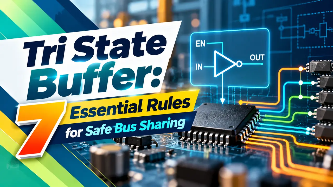
A tri state buffer is a logic buffer whose output can be high, low or high impedance, also called Z or the off state. When its enable input is active it copies the input to the output, and when disabled it electrically disconnects from the wire, as if it were not there at all.
An ordinary logic gate has only two output states, and it always drives one of them. That is fine for point to point wiring, but a shared data line needs a way for each chip to stop driving when another chip is talking.
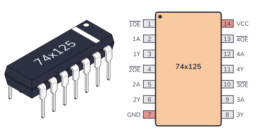
The pinout above is the 74HC125, a quad buffer with one enable per gate. Build Electronic Circuits shows the four output enable pins on pins 1, 4, 10 and 13, and notes that the HC version runs from 2 V to 6 V while the older 74LS125 needs 5 V.
How the High Impedance State Works
Inside a CMOS output there is a P channel MOSFET to the supply and an N channel MOSFET to ground. For a high output the top transistor is on, for a low output the bottom one is on, and in the Z state both are switched off together.
With both transistors off, the pin only shows a tiny leakage current and a few picofarads of capacitance. Nexperia specifies an off state output current of plus or minus 0.5 µA at 25 °C for the 74HC125, rising to plus or minus 5 µA over the industrial range up to 85 °C.
| Enable nOE | Input nA | Output nY | Meaning |
|---|---|---|---|
| L | L | L | Buffer active, drives low |
| L | H | H | Buffer active, drives high |
| H | X | Z | Disabled, high impedance |
This function table comes from the Nexperia 74HC125 datasheet, where X means the input does not matter. The small circle on the enable pin in the symbol shows that the enable is active low.
TRI STATE was originally a registered trademark of National Semiconductor for its three state logic products. Engineers now use the generic names three state, tri state and high Z for the same function.
Active Low and Active High Enable Types
Four buffers, each with its own active low enable.
Same pinout idea, but each enable is active high.
Eight buffers in two groups of four, each group with one enable.
Eight bidirectional channels with a direction pin and an enable.
The choice between active low and active high usually depends on the chip select logic. Many decoders produce active low outputs, which suit the 74HC125 and 74HC244 directly without extra inverters.
Every tri state buffer in these families has the same input logic levels as other HC parts. If you mix supply voltages, check the levels described in TTL vs CMOS logic families before connecting the bus.
Sharing a Bus Without Collisions
On a shared bus, every device output goes through a tri state buffer, and a control circuit makes sure only one enable is active at a time. This is how a microcontroller reads memory, input ports and peripherals over the same 8 data lines.
The receiving device normally captures the bus value with a clock edge in a latch or register. The data must be stable before that edge, so the enable time of the buffer is part of the timing budget.
Draw a simple timing chart of every enable signal before building a bus. If two enables overlap even for a few nanoseconds, add a small gap between one device releasing the bus and the next device driving it.
Bus Contention and Why It Damages Chips
Bus contention happens when two outputs drive the same line at the same time with opposite levels. One output tries to pull the line high while the other pulls it low, so a large current flows straight from the supply to ground through both output stages.
The line sits at some middle voltage that neither receiver can read reliably, and the output transistors heat up. Short events cause supply noise and ground bounce, while long events can permanently damage the drivers.
Common causes are overlapping chip selects and firmware that drives a pin while an external tri state buffer is also enabled. Nexperia lists about 15 ns typical enable and disable time for the 74HC125 at 4.5 V.
Floating Bus Lines and Pull Resistors
When every tri state buffer on a line is disabled, nothing drives the wire and it floats. A floating CMOS input can drift into the middle region, where both input transistors conduct partly, current rises and noise causes random switching.
The usual fix is a pull up or pull down resistor that holds the line at a known level when idle. The same idea is used on RS 485 networks, where biasing resistors keep the receiver in a known state when no node is transmitting.
Rise time 10 to 90 percent: t = 2.2 × R × C bus
ΔV = allowed voltage drop at the receiver
n = number of devices on the line, I leak = off state leakage each
Example:
n = 8, I leak = 5 µA, ΔV = 1.0 V
R max = 1.0 ÷ (8 × 5 µA) = 25 kΩ
With R = 10 kΩ and C bus = 50 pF:
t = 2.2 × 10 kΩ × 50 pF = 1100 ns
The resistor must be small enough that leakage cannot pull the line out of the valid logic range. The rise time matters only when the bus is idle, since an enabled driver is far faster.
Tri State Buffer Pull Resistor Calculator
The default leakage of 5 µA is the 85 °C maximum from the Nexperia datasheet. Add receiver input leakage to the total for extra margin.
Second Worked Example: A Slow Pull Up
Suppose an engineer picks 100 kΩ to save power on the same 8 device bus with 50 pF of capacitance. The calculator shows the maximum allowed value is 25 kΩ, so 100 kΩ could let leakage drag the idle level down by up to 4 V in the worst case.
The idle rise time also grows to 2.2 × 100 kΩ × 50 pF, which is 11000 ns or 11 µs. Firmware reading the bus soon after release may see a false low, so 10 kΩ is safer.
Some logic families offer bus hold inputs, such as the 74LVCH series, which weakly keep the last valid level on a floating line. They remove the need for many pull resistors but must not be used where a defined idle level is required.
Bidirectional Buses With the 74HC245
A one way buffer cannot pass data back, so two way buses use a transceiver, which is two tri state buffer paths back to back. The 74HC245 has a direction pin DIR that chooses A to B or B to A, and an active low output enable that disables both directions.
The direction must change only while the outputs are disabled, otherwise both sides can briefly drive each other. A processor with an ALU usually drives DIR from its read signal and the enable from the address decoder.
The SPI case is very common on PLC and instrument boards, where several chips share one MISO line, as explained in SPI vs I2C protocol comparison. I2C is different, because it uses open drain outputs with pull ups instead of a tri state buffer.
7 Essential Rules for Using a Tri State Buffer
The last rule matters because several outputs switching together draw sharp current pulses. Good layout practice from signal integrity in high speed PCB design keeps those pulses from upsetting nearby logic.
When a microcontroller pin shares a line with an external buffer, configure it as an input by default at reset. Change it to an output only after the external tri state buffer has been disabled.
- Many devices can share one set of bus wires.
- Saves pins, traces and connector contacts.
- Fast switching with full CMOS output drive.
- Easy isolation of a circuit for testing.
- Risk of bus contention if enables overlap.
- Idle lines float without a pull resistor.
- Enable timing adds to the bus timing budget.
- Leakage limits how large pull resistors can be.
Troubleshooting Shared Bus Faults
- Probe each enable line together with the data line on an oscilloscope.
- Look for middle level voltages that show two drivers fighting.
- Check for hot buffer packages after a few minutes of running.
- Confirm a pull resistor is fitted on every line that can float.
- Verify the transceiver DIR signal changes only while disabled.
- Measure supply ripple close to the bus drivers during transfers.
A line that reads random values when idle is almost always floating, while a line stuck near half the supply usually means contention. Noise problems that look similar are covered in noise reduction techniques for digital ICs, and the 74HC595 shift register is another familiar part with a tri state output enable pin.
Nexperia 74HC125 Datasheet
Tri State Buffer Video Lesson
Tri State Buffer FAQ
It is a buffer whose output can be high, low or high impedance. An enable input decides whether it drives the line or fully disconnects from it.
This lets several devices share the same bus wire safely and in turn. Only the enabled device drives the line, while every other output stays quietly in the high impedance state.
High impedance means both output transistors are switched off, so the pin neither sources nor sinks current. Only a tiny leakage and a few picofarads of capacitance remain.
The line voltage is then set by other drivers or by a pull resistor. Without either of them, the line simply floats at an undefined and noisy voltage.
Yes, each of its four buffers is enabled when its output enable pin is low. A high level on that pin puts the output in the high impedance state.
The 74HC126 offers the same function with active high enables. Choose between the two based on the polarity of the chip select signals on your board.
It is the condition where two outputs drive the same line at once with opposite levels. A large current then flows from the supply to ground through both drivers.
The line sits at a middle voltage and the chips heat up. Repeated contention can create supply noise, corrupt data and eventually damage the output stages.
A floating CMOS input can drift to a middle voltage where it draws extra current and switches randomly. A pull resistor holds the line at a clear logic level when idle.
Choose the value from the total leakage and the allowed voltage drop. For eight devices with 5 µA leakage each, 25 kΩ is the largest safe value.
A buffer passes data in one direction only. A transceiver such as the 74HC245 has two paths with a direction pin that selects which way data flows.
Its output enable disables both paths at once. Change the direction only while the outputs are disabled to avoid a brief fight between the two sides of the bus.
No, the I2C bus uses open drain outputs that can only pull the line low. Pull up resistors bring the line high when every device releases it.
SPI is different, since a slave data output enters the high impedance state when its chip select is inactive. That behaviour is a classic example of tri state use.
Related Articles
- Digital Logic Gates Explained
- TTL vs CMOS Logic Families
- Multiplexer vs Demultiplexer
- 74HC595 Shift Register
- SPI vs I2C Protocol Comparison
External References
- 74HC125 and 74HCT125 Quad Buffer, 3 State, Nexperia Datasheet
- 74HC125 and 74LS125 Explained, Build Electronic Circuits
- Three State Logic, Wikipedia
What We Learn Today
- A tri state buffer can drive high, drive low or disconnect into a high impedance state, which lets many chips share one bus line safely.
- Only one driver may be enabled at a time, because two outputs fighting over the same line create bus contention, heat and supply noise.
- Idle lines need a pull resistor, sized from total leakage and allowed voltage drop, or a bus hold input to avoid floating.