
The common emitter configuration is the most widely used BJT amplifier circuit -- providing voltage gain, current gain, and 180-degree phase inversion.
This guide covers the circuit, DC biasing, voltage gain calculation, and the role of each component -- with a live gain calculator.
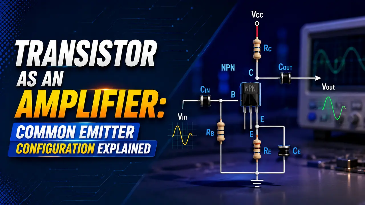
Input at the base, output at the collector -- the emitter is the shared (common) terminal for both circuits. Voltage gain = RC / re, where re is the dynamic emitter resistance of the transistor.
Common Emitter Amplifier: How the BJT Amplifies a Signal
A BJT amplifies because a small base current controls a much larger collector current. The gain β (beta) is the ratio of collector to base current.
In this configuration, current gain combined with the collector resistor produces voltage gain.
Three things determine how well the amplifier works in this configuration: the DC bias point (Q-point), the AC voltage gain, and the 180-degree phase inversion between input and output. Click any term to expand.
Common Emitter Amplifier Circuit Components
A practical CE amplifier circuit has six main components: the transistor, two biasing resistors (R1 and R2), a collector resistor (RC), an emitter resistor (RE), and two coupling capacitors (Cin and Cout). An emitter bypass capacitor (CE) is often added to increase AC gain.
| Component | Function | Typical Value |
|---|---|---|
| R1 (upper bias) | Forms voltage divider with R2 to set base voltage and Q-point | 10 kΩ to 100 kΩ |
| R2 (lower bias) | Forms voltage divider with R1; lower value sets higher base voltage | 2.2 kΩ to 22 kΩ |
| RC (collector) | Converts collector current changes into output voltage; sets AC gain | 1 kΩ to 10 kΩ |
| RE (emitter) | Provides thermal stability and negative feedback; reduces gain slightly | 100 Ω to 1 kΩ |
| CE (emitter bypass) | Short circuits RE for AC signals, restoring full AC gain while keeping DC stability | 10 µF to 100 µF |
| Cin (input coupling) | Blocks DC from the signal source; passes only the AC signal to the base | 1 µF to 10 µF |
| Cout (output coupling) | Blocks DC collector voltage from the load; passes only the AC output signal | 1 µF to 47 µF |
DC Biasing and the Q-point
The Q-point (quiescent point) is the DC operating point of the transistor with no AC signal applied. It must be set correctly for linear amplification.
Voltage divider biasing gives a stable base voltage independent of β. VE = VB minus 0.7 V.
IE ≈ VE / RE ≈ IC. Collector voltage VC = VCC minus IC × RC.
VE: emitter voltage = VB minus 0.7 V
IE: emitter current = VE / RE (≈ IC for high-β transistors)
VC: collector voltage = VCC minus IC × RC
Ideal: VC ≈ VCC / 2 for maximum undistorted output swing
Voltage Gain of the Common Emitter Amplifier
The AC voltage gain of this amplifier depends on the collector resistor and the transistor's dynamic emitter resistance. The dynamic emitter resistance re is a small-signal parameter -- it represents the AC resistance of the base emitter junction at the operating point.
RC: collector resistor (ohms)
re: dynamic emitter resistance = 26 mV / IC in milliamps
IC: quiescent collector current (mA)
With emitter bypass capacitor CE: Av = minus RC / re (full gain)
Without CE: Av = minus RC / (RE + re) ≈ minus RC / RE (reduced, stable gain)
Example: IC = 2 mA, RC = 4.7 kΩ, CE fitted.
re = 26 / 2 = 13 Ω. Av = 4700 / 13 = 362. Output is 362 times larger than input, inverted.
Without CE (RE = 470 Ω): Av = 4700 / 483 = 9.7. RE dramatically reduces gain but improves stability and reduces distortion.
This trade-off is the core design decision. See the BJT currents and voltages guide for how IC relates to β and IB.
Common Emitter Amplifier Calculator
Three BJT Amplifier Configurations Compared
| Parameter | Common Emitter | Common Collector (Emitter Follower) | Common Base |
|---|---|---|---|
| Input terminal | Base | Base | Emitter |
| Output terminal | Collector | Emitter | Collector |
| Common terminal | Emitter | Collector | Base |
| Voltage gain | High (RC/re) | Less than 1 (emitter follows base) | High (similar to CE) |
| Current gain | High (β) | High (β + 1) | Less than 1 (α) |
| Phase inversion | Yes (180°) | No | No |
| Input impedance | Medium (β × re) | High (β × RE) | Low (re) |
| Output impedance | High (≈ RC) | Low (≈ re) | High |
| Main use | General amplification, signal conditioning | Buffer, impedance matching | RF amplifier, current to-voltage |
Common Emitter Amplifier Applications
Audio Preamplifier
A microphone signal (typically a few millivolts) is amplified by one or more CE stages to line level. Each stage provides 20 to 40 dB of gain.
Coupling capacitors block DC between stages. See the RMS value guide.
Sensor Signal Amplification
Low level signals from thermocouples, strain gauges, and photodiodes are often too small for direct ADC input. A common emitter stage (or op-amp, which internally uses similar stages) amplifies the signal to a usable range. See the transistor basics guide for the underlying BJT operation.
Oscillator Feedback Stage
The CE amplifier is the gain element in RC phase-shift and LC oscillators. Its 180-degree phase inversion combines with another 180 degrees from the feedback network to satisfy the Barkhausen criterion.
See the reactance guide for how LC networks create phase shift.
Logic Level Interface
A CE stage converts a 3.3 V logic signal to a 12 V relay drive signal.
With RC sized for saturation, the transistor acts as a digital switch rather than a linear amplifier. See the semiconductor guide.
Watch: Common Emitter Transistor Amplifier Explained
Common Emitter Amplifier Questions
External References
- Common Emitter Amplifier and BJT Amplifier Circuits -- Electronics Tutorials
- Transistor Common Emitter Configuration -- Electronics Notes
What We Learn Today
- The common emitter stage takes input at the base, output at the collector, with the emitter as the common terminal
- Voltage gain Av = RC / re (with CE bypass) or RC / (RE + re) without CE -- always with 180-degree phase inversion
- Dynamic emitter resistance re = 26 mV / IC(mA) -- the key parameter linking collector current to AC voltage gain
- Voltage divider biasing (R1, R2) sets a stable Q-point at VCC / 2 for maximum output swing
- The emitter bypass capacitor CE increases AC gain while RE maintains DC stability -- a fundamental design trade-off
- Common emitter is used in audio preamps, sensor signal amplifiers, oscillator feedback stages, and logic interface circuits