
What Is a Bipolar Junction Transistor (BJT)?
A Bipolar Junction Transistor, commonly known as a BJT, is a three terminal semiconductor device used to amplify electrical signals and switch electronic circuits. It consists of two PN junctions arranged as either an NPN or PNP transistor. Unlike field effect transistors that are voltage controlled, a BJT is a current controlled device, meaning a small current flowing into the base terminal controls a much larger current flowing between the collector and emitter.
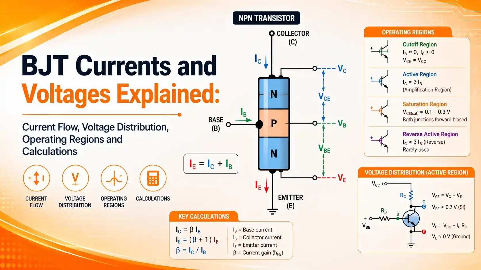
BJTs are widely used in audio amplifiers, relay driver circuits, power supplies, oscillators, industrial control systems and embedded electronics. Despite the growing popularity of MOSFETs, BJTs continue to be preferred in many analog applications because of their excellent linearity, predictable current gain and cost effectiveness.
- Audio amplifiers
- Relay driver circuits
- Motor driver circuits
- Switch mode power supplies
- Oscillator circuits
- PLC interface modules
- Instrumentation electronics
- Sensor signal conditioning
If you are new to semiconductor devices, you may also enjoy our article on What Is a Semiconductor?, which explains how PN junctions form the foundation of diodes and transistors. Understanding PN junction behavior will make BJT operation much easier to understand.
Think of the base terminal as a control valve. A very small base current regulates a much larger collector current, making the transistor an efficient electronic amplifier and switch.
BJT Construction and Terminals
A Bipolar Junction Transistor consists of three semiconductor regions known as the Emitter, Base and Collector. These regions are formed by doping semiconductor material to create two PN junctions. Depending on the arrangement of these regions, the transistor is classified as either an NPN transistor or a PNP transistor.
The emitter is heavily doped so that it can inject a large number of charge carriers into the base region. The base is extremely thin and lightly doped, allowing most of these carriers to pass through with minimal recombination. The collector is moderately doped and physically larger because it must dissipate more heat while collecting charge carriers from the emitter.
NPN Transistor
An NPN transistor consists of a P type base sandwiched between two N type semiconductor layers. It is the most widely used BJT because electrons, which are the majority charge carriers, move faster than holes. NPN transistors are commonly used in amplifiers, switching circuits and digital electronics.
- Majority carriers are electrons.
- Turns ON when the base is positive with respect to the emitter.
- Current flows from collector to emitter.
- Most common transistor in practical circuits.
PNP Transistor
A PNP transistor consists of an N type base between two P type semiconductor regions. It operates in the opposite manner to an NPN transistor. The base must be negative with respect to the emitter for conduction to occur.
- Majority carriers are holes.
- Turns ON when the base becomes negative.
- Current flows from emitter to collector.
- Used where positive supply switching is required.
| Feature | NPN | PNP |
|---|---|---|
| Charge Carrier | Electrons | Holes |
| Base Bias | Positive | Negative |
| Current Direction | Collector → Emitter | Emitter → Collector |
| Popularity | Very High | Moderate |
BJT Current Flow Explained
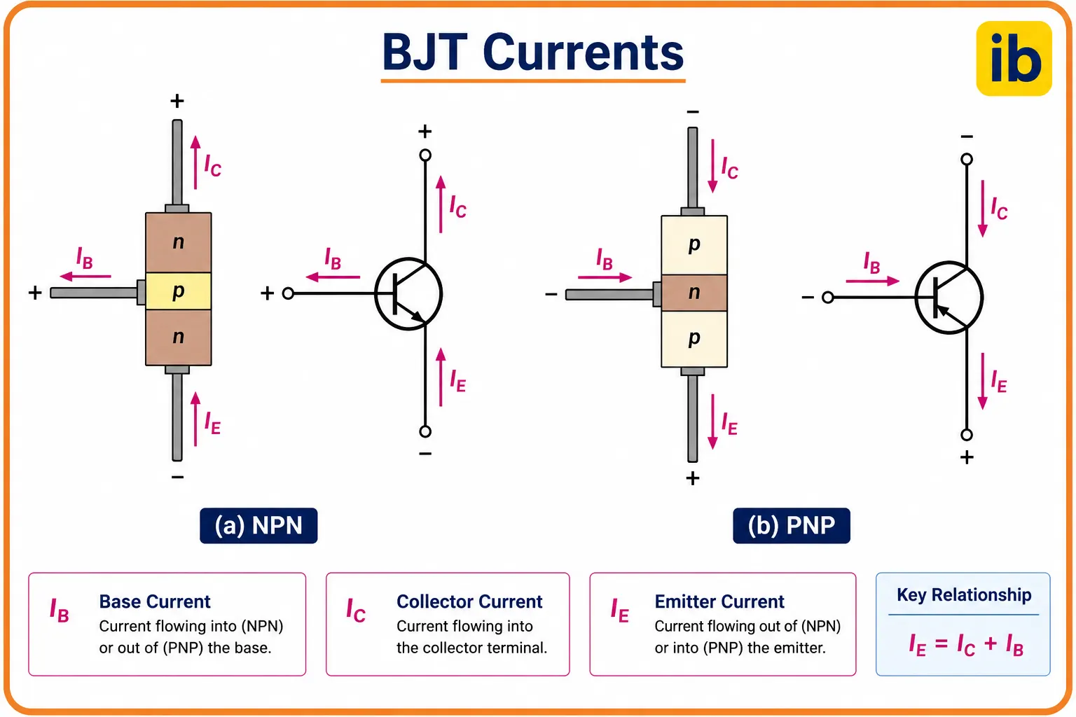
The operation of a Bipolar Junction Transistor is based on the movement of charge carriers through its three terminals. Although three different currents exist inside the transistor, they are directly related and obey one of the most important current equations in electronics.
The emitter injects charge carriers into the thin base region. Since the base is lightly doped and extremely thin, only a very small percentage of carriers recombine inside it, producing a small base current. The remaining carriers continue into the collector region, producing the much larger collector current.
The emitter current is always the largest current because it supplies both the collector current and the base current.
The Three BJT Currents
Emitter Current (IE)
The emitter current is the total current supplied by the emitter terminal. It is the largest current inside the transistor because it divides into collector current and base current.
Collector Current (IC)
Collector current carries almost all of the emitter current through the transistor. It is responsible for driving the external load and producing amplification.
Base Current (IB)
Base current is very small compared with collector current. Its primary purpose is to control transistor operation.
BJT Current Relationships
Kirchhoff's Current Law applies directly to transistor operation. Since current entering a junction must equal the current leaving the junction, the emitter current is always equal to the sum of the collector current and base current.
These three equations are fundamental to transistor analysis and are used extensively when designing amplifiers, electronic switches and industrial control circuits. If you are unfamiliar with current calculations, our article on Ohm's Law Explained provides an excellent foundation for understanding circuit behavior.
If the transistor has a current gain (β) of 100, a base current of only 1 mA can control a collector current of approximately 100 mA. This ability to amplify current is what makes BJTs extremely useful in analog and digital electronic circuits.
BJT Voltage Relationships
Understanding the voltage at each transistor terminal is just as important as understanding current flow. The operating state of a Bipolar Junction Transistor depends on the voltage differences between the collector, base and emitter terminals. These voltages determine whether the transistor behaves as an amplifier, an electronic switch or remains completely turned off.
For an NPN transistor operating in the active region, the base emitter junction is forward biased while the collector base junction remains reverse biased. Under these conditions, a small change in base current produces a much larger change in collector current, allowing the transistor to amplify electrical signals.
Base Voltage (VB)
The base voltage controls transistor conduction. For a silicon transistor, the base is typically about 0.7 V higher than the emitter during normal operation.
Emitter Voltage (VE)
The emitter serves as the reference terminal in many transistor circuits. Its voltage depends on circuit configuration and emitter resistor values.
Collector Voltage (VC)
The collector voltage changes according to collector current and load resistance. It is usually the output terminal in common emitter amplifier circuits.
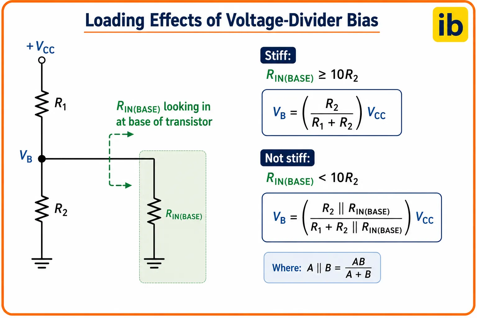
| Parameter | Typical Value |
|---|---|
| Base Emitter Voltage (VBE) | Approximately 0.7 V |
| Collector Emitter Saturation Voltage (VCE(sat)) | Approximately 0.2 V |
| Base Collector Junction | Reverse Biased |
BJT Operating Regions
Depending on the applied voltages, a Bipolar Junction Transistor operates in one of three primary regions. Each region has a different purpose in electronic circuit design.
The transistor is OFF because the base emitter junction is not forward biased. Collector current is essentially zero, making this region suitable for electronic switching applications.
The transistor behaves as a linear amplifier. The collector current is proportional to the base current, making this the preferred operating region for analog signal amplification.
Both PN junctions become forward biased. The transistor behaves like a closed switch with very little voltage drop across the collector emitter terminals.
- Cutoff Region = Switch OFF
- Active Region = Amplifier
- Saturation Region = Switch ON
Practical Example of BJT Current Calculation
Consider an NPN transistor with a current gain (β) of 120. If the base current is 0.5 mA, the collector current and emitter current can be calculated using the transistor current equations.
IB = 0.5 mA
IC = 120 × 0.5
IC = 60 mA
IE = 60 + 0.5
IE = 60.5 mA
These calculations are performed routinely when designing transistor amplifiers, relay driver circuits and switching interfaces for microcontrollers and PLC systems. Before selecting resistor values, engineers often apply Ohm's Law to determine the required base current and bias voltages.
The value of β is not fixed. It varies with transistor type, operating current, temperature and manufacturer. Always use the minimum guaranteed current gain from the transistor datasheet when designing reliable switching circuits.
Common BJT Configurations
BJTs can be connected in three basic circuit configurations. Each configuration provides different electrical characteristics and is selected according to the application requirements.
| Configuration | Input | Output | Main Application |
|---|---|---|---|
| Common Emitter | Base | Collector | Voltage and current amplification |
| Common Collector | Base | Emitter | Buffer amplifier and impedance matching |
| Common Base | Emitter | Collector | High frequency amplification |
Industrial Applications of BJTs
Although MOSFETs dominate many modern power electronic applications, Bipolar Junction Transistors continue to play an important role in analog electronics and industrial control systems. Their excellent current gain, predictable characteristics and low cost make them suitable for numerous amplification and switching applications.
Audio Amplifiers
BJTs provide high quality signal amplification in microphone preamplifiers, audio amplifiers and communication equipment where linear operation is essential.
Relay Driver Circuits
Microcontrollers and PLC outputs cannot directly energize many industrial relays. BJTs act as electronic switches that safely drive relay coils using a small control current.
Motor Driver Circuits
Small DC motors, cooling fans and actuator circuits frequently use BJTs as low cost switching devices.
Power Supplies
Linear voltage regulators and reference circuits commonly use transistors for voltage regulation and current control.
Oscillator Circuits
Many oscillator and waveform generation circuits rely on transistor amplification to sustain oscillations.
Instrumentation Electronics
Signal conditioning circuits, analog sensors and measurement equipment often use BJTs because of their excellent linear characteristics.
Inside a PLC control panel, a transistor may receive only a few milliamperes from the controller output while switching a relay that controls an industrial motor starter carrying several amperes. This demonstrates how a very small control current can safely manage much larger electrical loads.
BJT Advantages and Limitations
Advantages
- High current gain
- Excellent analog amplification
- Low manufacturing cost
- Good linear operating characteristics
- Simple circuit design
- Widely available
- Suitable for low power applications
Limitations
- Requires continuous base current
- Lower input impedance than MOSFETs
- Higher power consumption
- Current gain varies with temperature
- Slower switching than many MOSFETs
- Thermal runaway is possible without proper design
BJT vs MOSFET
BJTs and MOSFETs are both semiconductor devices used for amplification and switching, but they operate using different control mechanisms. Understanding their differences helps engineers choose the most appropriate device for a particular application.
| Feature | BJT | MOSFET |
|---|---|---|
| Control Method | Current Controlled | Voltage Controlled |
| Input Impedance | Lower | Very High |
| Drive Power | Requires Base Current | Minimal Gate Current |
| Switching Speed | Moderate | High |
| Linear Amplification | Excellent | Good |
| Typical Applications | Amplifiers, Drivers | Power Electronics, SMPS, Motor Drives |
Choose a BJT when accurate analog amplification and predictable current gain are important. Choose a MOSFET when high switching speed, high efficiency and very low input drive power are required.
Common Design Mistakes
Many transistor circuits fail because of incorrect biasing or improper component selection rather than defective transistors. Understanding these common mistakes helps engineers design more reliable electronic circuits.
Ignoring Base Resistors
Connecting the base directly to a voltage source can permanently damage the transistor because excessive base current may flow.
Assuming β Is Constant
Current gain varies between transistor devices and changes with operating conditions. Always design using datasheet minimum values.
Poor Heat Management
Power transistors generate heat. Inadequate cooling can lead to excessive junction temperature and device failure.
Wrong Operating Region
Amplifiers should operate in the active region, while switching circuits should alternate between cutoff and saturation.
Incorrect Pin Connections
Emitter, base and collector terminals differ between transistor packages. Always verify the pin configuration before installation.
No Flyback Diode
When switching inductive loads such as relays or solenoids, always install a flyback diode to protect the transistor from voltage spikes.
- Verify transistor pin configuration.
- Calculate the required base resistor.
- Check collector current rating.
- Confirm power dissipation limits.
- Ensure adequate heat sinking if required.
- Verify operating region.
- Protect inductive loads with a flyback diode.
- Review the manufacturer datasheet before finalizing the design.
Related Articles on InstrumentationBlog
Continue your journey into electronics and electrical engineering with these carefully selected articles. They complement the concepts discussed in this guide and provide a deeper understanding of semiconductor devices, circuit analysis and industrial automation.