
Two matched transistors and one resistor can hold a steady current into almost any load, and that trick sits inside nearly every analog IC.
A mirror circuit sets a reference current in one transistor and forces a second transistor to copy it. It replaces resistors for biasing, active loads and constant current sources in amplifiers and ICs.
What Is a Current Mirror?
A current mirror is a circuit that copies the current flowing in a reference transistor into one or more output transistors, holding that output current nearly constant as the load voltage changes. The simplest version uses two matched BJTs whose base emitter junctions share the same voltage, a relationship explained in BJT currents and voltages.
All About Circuits explains that holding VBE constant holds the emitter current constant. The collector current through the load is therefore regulated.
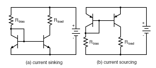
An NPN version sinks current from a load tied to the positive supply. A PNP version sources current into a load tied to ground.
Mirrors are the standard way to bias the differential amplifier stage inside every op amp. They also act as active loads that give very high gain.
How the Basic Current Mirror Works
Q1 is diode connected, so its VBE adjusts itself to carry the reference current. Q2 has the identical VBE and, if matched, carries the same collector current.
All About Circuits stresses that both transistors must share the same temperature. Discrete designs glue the cases together, while ICs place them side by side on one die.
Current Mirror Formulas
I out = I ref × β ÷ (β + 2)
With Early effect: I out ≈ I out × (1 + (VCE2 minus VCE1) ÷ VA)
Worked example:
VCC = 12 V, VBE = 0.7 V, R = 11.3 kΩ, I ref = 1.00 mA
β = 100, I out = 1.00 × 100 ÷ 102 = 0.980 mA
VA = 100 V, VCE2 = 5 V, VCE1 = 0.7 V
I out ≈ 0.9804 × 1.043 ≈ 1.023 mA
The first error comes from the two base currents taken from the reference. The second comes from the Early effect, which makes collector current rise slowly with VCE.
The output stays valid only while Q2 is out of saturation, typically above about 0.2 V to 0.3 V. This limit is called the compliance voltage.
5 Proven Current Mirror Designs
The cascode idea is the same one used in the cascode amplifier. It trades extra headroom for a much flatter output current.
A Widlar mirror adds an emitter resistor on the output side to create very small currents without huge resistors. It is common in op amp input stages.
BJT vs MOSFET Mirrors
| Feature | BJT Mirror | MOSFET Mirror |
|---|---|---|
| Set by | Matched VBE | Matched VGS |
| Ratio control | Emitter area | W ÷ L ratio |
| Base or gate current error | Yes | None |
| Output resistance | VA ÷ I | 1 ÷ (λ × I) |
| Minimum output voltage | About 0.2 V | VGS minus Vth |
In CMOS chips, the mirror ratio is set by transistor width and length. The basics of the device are covered in MOSFET working principle.
Several outputs can share one reference, each scaled by its size. All About Circuits shows multiple mirrors driven from one reference transistor and resistor.
Where a Current Mirror Is Used
Constant current excitation is one reason mirror stages appear in 4 to 20 mA instrumentation circuits. Matched strings also keep LED brightness uniform.
Mirror Output Calculator
Raise VA or lower the output VCE to see the error shrink. A Wilson or cascode stage cuts it further.
- Precise, stable bias currents.
- Few components.
- High output resistance.
- Easy to scale and copy.
- Needs well matched transistors.
- Base current and Early errors.
- Limited output voltage swing.
- Temperature gradients cause mismatch.
Georgia Tech Mirror Notes PDF
BJT Mirror Explained Video
Current Mirror FAQ
Related Articles
- BJT Currents and Voltages
- Differential Amplifier and CMRR
- Cascode Amplifier
- Op Amp Basics
- Common Emitter Amplifier
External References
What We Learn Today
- Matched VBE lets one transistor copy the reference current.
- Base current and Early effect set the main errors.
- Wilson, Widlar and cascode designs improve accuracy.