
Both semiconductors leave ordinary silicon behind, yet they dominate almost entirely different corners of power electronics. Here is exactly how silicon carbide and gallium nitride differ, with a real power-versus-frequency chart and a live selection tool you can try right now.
What Are Wide-Bandgap Semiconductors?
Silicon carbide and gallium nitride are both wide-bandgap semiconductors, materials that need far more energy to conduct than ordinary silicon, and that extra headroom translates directly into higher voltage, higher temperature, and higher frequency capability.
Both materials have effectively taken over roles that older silicon devices, including the thyristors and triacs we covered previously, once handled on their own, wherever the application demands more efficiency than legacy silicon can deliver.
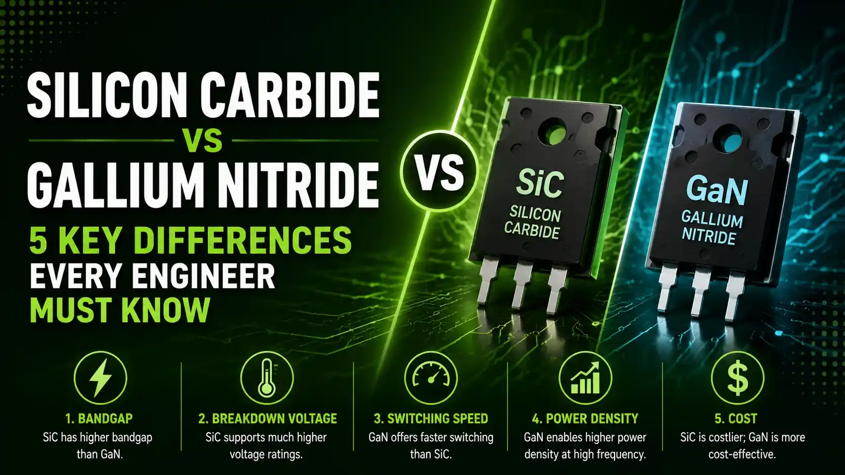
This guide covers the five key differences between silicon carbide and gallium nitride, from raw material properties to why each one has carved out such a distinct place in modern power electronics.
Neither material is simply a drop-in upgrade for the other, despite both getting grouped together under the same "wide-bandgap" label. A design team choosing between them is really choosing between two different sets of trade-offs, not picking the objectively better option, and that distinction matters more the closer a project sits to the boundary between their respective sweet spots.

Silicon Carbide vs Gallium Nitride: Core Definitions
Before comparing the details, it helps to see each material's basic identity side by side.
Silicon Carbide (SiC)
A compound of silicon and carbon with excellent thermal conductivity, capable of blocking very high voltages while running hot without breaking down.
Best for: high-power, high-voltage applications like EV traction inverters and solar farms.
Gallium Nitride (GaN)
A compound of gallium and nitrogen with exceptionally high electron mobility, enabling extremely fast switching at lower to moderate voltages.
Best for: high-frequency, compact designs like fast chargers and RF power amplifiers.
5 Key Differences Between Silicon Carbide and Gallium Nitride
These five differences explain why silicon carbide and gallium nitride, despite both being wide-bandgap materials, end up serving such different parts of the power spectrum.
Bandgap and Breakdown Field Are Both High, But Not Identical
Silicon carbide's bandgap sits around 3.3 eV with a breakdown field of roughly 2 to 4 MV/cm. Gallium nitride runs slightly higher at around 3.4 eV and about 3.3 MV/cm. Both dwarf silicon's 1.1 eV and 0.3 MV/cm, but the numbers are close enough that this alone rarely decides between them.
Gallium Nitride Switches Dramatically Faster
Gallium nitride's electron mobility, roughly 1500 to 2000 cm²/Vs, is more than double silicon carbide's 650 to 900 cm²/Vs. That difference is exactly why GaN dominates high-frequency switching applications where SiC struggles to keep up.
Silicon Carbide Handles Heat and Power Density Better
Silicon carbide's thermal conductivity, around 4.9 W/cm·K, comfortably beats gallium nitride's 1.3 to 2.2 W/cm·K. That single property is why SiC dominates the highest power, highest heat applications where GaN would struggle to keep cool.
Their Voltage and Power Ranges Barely Overlap
Commercial GaN devices generally top out around 650V and roughly 10kW. Commercial SiC devices routinely reach 1200V and beyond, scaling from around 1kW up into the megawatts. Each material effectively owns its own end of the power spectrum.
Manufacturing Maturity and Process Differ Sharply
SiC boules must be grown at temperatures above 2700°C, roughly 200 times slower than silicon, and the resulting wafers are thin and brittle. GaN, by contrast, can often be grown epitaxially on existing silicon substrates at 1000 to 1200°C, letting it lean on established silicon fabrication infrastructure.
Real Material Property Comparison
Rather than a redrawn summary, here are the actual published material properties behind every difference above.
| Property | Silicon (Si) | Silicon Carbide (SiC) | Gallium Nitride (GaN) |
|---|---|---|---|
| Bandgap (eV) | 1.12 | 3.3 | 3.44 |
| Breakdown Field (MV/cm) | 0.3 | 2 to 4 | 3.3 |
| Electron Mobility (cm²/Vs) | 1000 to 1400 | 650 to 900 | 1500 to 2000 |
| Saturation Velocity (x10⁷ cm/s) | 1.0 | 2.0 | 2.2 |
| Thermal Conductivity (W/cm·K) | 1.5 | 4.9 | 1.3 to 2.2 |
Data compiled from published EDN and industry sources, referenced below.
What is happening: A wider bandgap requires more thermal energy to knock an electron loose, which is exactly why SiC and GaN devices can operate at higher voltages and temperatures without the runaway conduction that would destroy a silicon device.
A real example: A silicon device with a 0.3 MV/cm breakdown field needs roughly ten times more material thickness to block the same voltage as an SiC or GaN device with a 3+ MV/cm rating, directly explaining why wide-bandgap devices can be so much smaller for the same voltage rating.
Why it works: Thinner material also means lower resistance and lower switching losses, which is the underlying reason both SiC and GaN deliver higher efficiency than silicon, just through two different material property advantages.
It is worth noting that these numbers describe idealized material properties, not finished devices. Real packaged parts also depend heavily on gate driver design, packaging parasitics, and thermal management, all of which can narrow or widen the practical gap between what a datasheet promises and what a circuit actually achieves in the field.
Try It: SiC vs GaN Application Selector
Set your target voltage and switching frequency to see which wide-bandgap technology real designs typically choose.
Manufacturing: Why the Two Materials Are Made So Differently
Silicon Carbide Manufacturing
SiC boules are grown at temperatures exceeding 2700°C, roughly 200 times slower than silicon crystal growth. The resulting wafers are nearly 50% thinner than silicon wafers and notably brittle, requiring specialized handling equipment throughout production.
Gallium Nitride Manufacturing
GaN is typically grown epitaxially on a host substrate, often silicon, silicon carbide, or sapphire, at 1000 to 1200°C. GaN-on-silicon in particular can piggyback on existing high-volume silicon fabrication lines, a real cost advantage at scale.
That manufacturing gap shows up directly in wafer pricing history. A 6-inch SiC wafer cost roughly $3,000 back in 2018, and even after years of steady improvement it still commands a real premium over silicon. GaN devices carry their own premium too, but the ability to reuse standard silicon-processing equipment has let costs fall faster in some segments, particularly for GaN-on-silicon parts aimed at consumer chargers and lower-power converters.
None of this means one technology is simply winning the cost race outright. Wafer size scaling, higher production volumes, and improved yields are pushing prices down on both sides at once, and the relative gap that exists today is very likely to keep shifting as both supply chains mature further over the coming years.
Real Application Roles Compared
Click each tab to see how SiC and GaN show up in genuinely different real-world systems.
SiC MOSFETs have increasingly replaced silicon IGBTs in EV traction inverters, since Tesla's move to an all-SiC Model 3 inverter helped popularize the shift. SiC's thermal conductivity and voltage headroom fit this high-power role well.
GaN's high switching frequency lets USB-C fast chargers and laptop adapters shrink dramatically in size while improving efficiency, which is exactly why GaN chargers have become common consumer products.
Solar inverters benefit from SiC's high voltage handling and low switching losses at the power levels typical of commercial and utility-scale solar installations.
GaN's exceptional high-frequency performance makes it a natural fit for RF power amplifiers in 5G base stations and radar systems, building on its earlier role in III-V compound semiconductor RF devices.
SiC vs GaN Comparison Table
| Feature | Silicon Carbide (SiC) | Gallium Nitride (GaN) |
|---|---|---|
| Typical Voltage Range | 600V to 1200V+ | 30V to 650V |
| Typical Power Range | 1kW to megawatts | Up to about 10kW |
| Switching Frequency | kHz to low MHz | Up to GHz range |
| Thermal Conductivity | High | Moderate |
| Manufacturing Maturity | Established, commercialized since 2010 | Growing rapidly, leverages Si infrastructure |
Applications of Silicon Carbide and Gallium Nitride
EV Traction Inverters
SiC MOSFETs convert battery DC into the AC that drives electric vehicle motors.
Fast Chargers
GaN enables compact, efficient USB-C and laptop chargers running at high frequency.
Solar and Renewable Inverters
SiC's voltage headroom suits utility-scale solar and wind power conversion.
Data Center Power Supplies
Both materials appear in AI data center power delivery, each suited to different stages.
5G and RF Power Amplifiers
GaN's high-frequency performance drives modern base station and radar amplifiers.
Industrial Motor Drives
SiC improves efficiency and shrinks passive components in industrial power conversion.
Notice how cleanly these six roles split along the same line drawn earlier: whichever application needs to push serious power through a small, hot package leans toward SiC, and whichever application needs blistering switching speed in a compact footprint leans toward GaN. Very few designs genuinely need both extremes at once, which is exactly why the two materials have settled into such distinct niches rather than displacing each other outright.
Advantages and Limitations of Each Technology
Why Silicon Carbide Leads at High Power
Where Gallium Nitride Pulls Ahead
Download Wide-Bandgap Semiconductor References
These two official references go deeper into real device selection between silicon, SiC, and GaN.
Power Analog Design Journal: GaN and SiC Power Applications
Official Texas Instruments journal comparing IGBT, SiC, and GaN devices
Power System Topology Selection Guide: Si, SiC, GaN
Official Infineon guide for choosing between the three power semiconductor families
Watch: Wide-Bandgap SiC and GaN Devices Explained
This lecture from the University of Cambridge covers wide-bandgap device characteristics and applications.
FAQs on Silicon Carbide vs Gallium Nitride
External References
- EDN, GaN vs SiC: A Look at Two Popular WBG Semiconductors in Power
- Texas Instruments, Power Analog Design Journal, 4Q 2020
- Infineon, Power System Topology Selection Guide
- YouTube, University of Cambridge, Wide Bandgap SiC and GaN Devices
What we learn today
- Silicon carbide and gallium nitride are both wide-bandgap semiconductors, but their specific properties differ enough to send them to opposite ends of the power spectrum.
- Gallium nitride's much higher electron mobility gives it a decisive switching-speed advantage over silicon carbide.
- Silicon carbide's superior thermal conductivity makes it the practical choice for the highest power, highest voltage applications.
- Commercial voltage ranges barely overlap: GaN tops out near 650V, while SiC comfortably exceeds 1200V.
- Manufacturing processes differ sharply, SiC demands extreme, slow crystal growth, while GaN can often reuse existing silicon fabrication infrastructure.