
An ADC needs a steady voltage while it converts, yet real signals keep moving during those few microseconds. A small switch, a capacitor and two buffers freeze the input for long enough to give every conversion a trustworthy value.
Successive approximation and many other converters need a frozen input while they work. A well designed sample and hold stage captures the signal at a precise instant and keeps it steady until conversion ends.
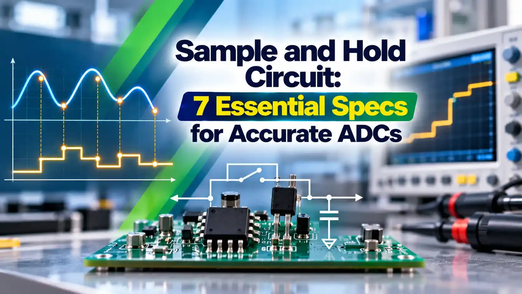
What Is a Sample and Hold Circuit?
A sample and hold circuit is an analog stage that tracks an input voltage and then, on command, freezes it on a capacitor so that a converter can measure a constant value. It sits at the front of most analog to digital conversion systems.
Electronics Hub describes the basic circuit as two parts, an analog switch and a holding capacitor. When the switch closes the capacitor follows the input, and when it opens the capacitor keeps the last voltage.
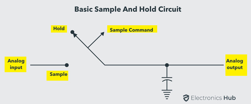
Electronics Hub also notes that two buffers, one at the input and one at the output, are added so the source can charge the capacitor quickly and the load cannot drain it. These buffers are usually op amp voltage followers.
Many engineers say track and hold instead, because the output follows the input continuously during the sample phase. Analog Devices uses the term SHA, short for sample and hold amplifier, for both kinds.
Why ADCs Need a Frozen Input
A successive approximation converter compares the input with a trial value one bit at a time, as explained in ADC working principle. If the input changes by more than half an LSB during those comparisons, the result can be wrong by many codes.
For a 12 bit converter with a 10 V range, one LSB is 2.44 mV. A 1 kHz sine wave of full amplitude moves faster than that in under 100 nanoseconds near zero crossing, so the input must be frozen.
Modern SAR chips include the sample and hold inside, usually as a switched capacitor array. Even so, the external driver must charge that internal capacitor in time, which is why the same specifications still matter when reading a PLC analog input datasheet.
How the Circuit Works, Step by Step
The switch is usually a JFET or MOSFET, as Electronics Hub explains, and it can be placed in series or in shunt with the signal. The behaviour of such devices is covered in types of electronic switches.
Drive the hold control from a clean, low jitter clock, not from a busy microcontroller pin. A noisy edge moves the sampling instant and shows up as extra noise on fast signals.
7 Essential Sample and Hold Specifications
| Specification | Meaning | Main Cause |
|---|---|---|
| Acquisition time | Time to track a new input to a stated accuracy | Buffer slew, switch resistance, capacitor size |
| Aperture time | Delay for the switch to open after hold command | Switch and driver speed |
| Aperture jitter | Sample to sample variation of that delay | Clock and switch noise |
| Hold mode settling | Time for output to settle after switching | Transient recovery of buffers |
| Droop rate | Change of held voltage per unit time | Leakage and bias currents |
| Hold step or pedestal | Offset dumped onto capacitor at switch off | Switch charge injection |
| Feedthrough | Input signal leaking to output during hold | Stray capacitance across switch |
Analog Devices tutorial MT 090 defines acquisition time as the interval needed to reacquire the signal to the desired accuracy when switching from hold to track, usually quoted at 0.1 and 0.01 percent. It is measured from the 50 percent point of the sampling clock edge.
The same tutorial explains that droop caused by reverse biased junction leakage roughly doubles for every 10 °C rise in temperature. A design that is fine on the bench can therefore fail inside a hot panel.
MT 090 adds that typical devices show aperture jitter below 50 ps rms, while high speed devices reach below 5 ps rms. Feedthrough becomes a problem when it exceeds half an LSB at the input frequency of interest.
Acquisition Time and Droop Formula
A simple single pole model treats the switch and buffer output resistance R as charging the hold capacitor C. To settle within half an LSB of an N bit converter, the capacitor needs about RC times ln of 2 to the power N plus 1.
Droop voltage ΔV = I leakage × t hold ÷ C
LSB = Full scale ÷ 2^N
Example:
R = 200 Ω, C = 1 nF, N = 12 bits
RC = 0.2 µs, ln(8192) = 9.01
t = 0.2 × 9.01 = 1.80 µs
I = 1 nA, hold 10 µs: ΔV = 1 × 10 ÷ 1 = 10 µV
LSB = 10 V ÷ 4096 = 2441 µV, so droop = 0.0041 LSB
Real parts also need time for the buffer to slew, so treat this result as a minimum. The LF398 datasheet quotes about 4 µs to 0.1 percent with 1000 pF, which includes its own amplifier limits.
Acquisition and Droop Calculator
Second Worked Example: Aperture Jitter Budget
A sampling instant that wanders by tj seconds produces an error equal to tj times the slope of the signal. For a full scale sine wave of frequency f, keeping that error under half an LSB requires tj below 1 ÷ (2^(N+1) × π × f).
For a 12 bit system sampling a 100 kHz sine, tj must be below 1 ÷ (8192 × 3.1416 × 100000), which is about 389 ps. At 1 MHz the limit drops to about 39 ps, so clock quality starts to dominate.
The same jitter also sets a ceiling on signal to noise ratio, equal to minus 20 log of 2π f tj. Use the SNR calculator to compare that limit with the ideal 6.02 N plus 1.76 dB of the converter.
Aperture jitter error grows with input frequency, not with sampling rate. A slow sampling system that captures fast signals, such as an undersampling receiver, still needs a very clean clock.
Choosing the Hold Capacitor
The hold capacitor sets the main trade off of every hold circuit design. A large value gives low droop and a small hold step, while a small value gives fast acquisition.
Very low dielectric absorption and leakage.
Low absorption, wide availability, good stability.
Lowest absorption and works at high temperature.
Stable small values with low absorption.
High absorption, leakage and voltage dependence.
The LF398 datasheet lists polystyrene, polypropylene and Teflon as dielectrics with very low hysteresis, and MT 090 recommends mica, polystyrene and polypropylene while warning against electrolytic and some high K ceramics. The reasons are explained in capacitor types and capacitor failure modes.
Guard the hold capacitor node with a ring of copper driven by the output buffer, and keep it away from digital traces. Surface leakage on a dusty or humid board can exceed the leakage of the switch itself.
The LF398 Monolithic Hold IC
The Texas Instruments LF398 combines input buffer, switch and output buffer in one 8 pin package, needing only an external hold capacitor. It runs from ±5 V to ±18 V supplies, with ±15 V recommended.
Its datasheet quotes acquisition of about 4 µs with 1000 pF and about 20 µs with 0.01 µF, both to 0.1 percent. With a 1 µF capacitor the droop rate is about 5 mV per minute.
The hold step is typically 0.5 to 2.5 mV with 0.01 µF, and feedthrough rejection is 80 to 96 dB at 1 kHz depending on grade. Its 10¹⁰ Ω input impedance suits high impedance sources and precision rectifier outputs.
- Freezes fast signals for accurate conversion.
- Lets one ADC serve many channels through a multiplexer.
- Allows simultaneous sampling of several channels.
- Captures peaks and transients at an exact instant.
- Droop limits how long a value can be held.
- Hold step adds an offset that needs calibration.
- Aperture jitter limits high frequency accuracy.
- Capacitor choice trades speed against hold accuracy.
Design and Selection Steps
In multichannel systems a multiplexer often feeds a single sample and hold, and switching transients from the multiplexer must settle before the hold command. Simultaneous sampling uses one stage per channel and holds them together, which keeps phase relationships correct.
Troubleshooting Hold Errors
- Measure droop by holding a known DC level and timing the change.
- Check the hold step with the input grounded.
- Confirm the hold capacitor dielectric and voltage rating.
- Clean flux residue around the hold node and guard ring.
- Verify the control edge is clean and fast.
- Check that the input buffer can drive the capacitor without oscillating.
- Watch for feedthrough with a large input during hold.
A slow tail after each acquisition often points to dielectric absorption, while a steady offset points to hold step. Noise picked up on the hold node is reduced by a solid ground and by the measures in electromagnetic interference control.
Where These Circuits Are Used
Analog Devices MT 090 Tutorial
Op Amp Track and Hold Video
Sample and Hold FAQ
It is an analog stage that tracks an input voltage and then freezes it on a capacitor. The frozen value stays steady while a converter measures it.
The basic parts are an analog switch, a hold capacitor and two buffers. The buffers let the source charge the capacitor quickly and stop the load from draining it.
It is the time the stage needs to track a new input to a stated accuracy after switching from hold to track. Analog Devices usually quotes it at 0.1 and 0.01 percent.
It depends on buffer slew rate, switch resistance and the hold capacitor value. A larger capacitor gives a longer acquisition time for the same circuit.
Droop comes from leakage currents in the switch, the capacitor and the output buffer bias current. These small currents slowly charge or discharge the held voltage on the capacitor.
Junction leakage roughly doubles with every 10 degree rise in temperature. Using a larger capacitor, a low leakage switch or a cooler location reduces the droop rate.
It is the random variation in the exact moment the switch opens from one sample to the next. The error it causes equals the jitter multiplied by the slope of the signal.
Fast changing inputs therefore suffer more than slow ones. Typical parts show below 50 picoseconds rms, and high speed parts go below 5 picoseconds.
Polypropylene, polystyrene and Teflon film capacitors have very low dielectric absorption and very low leakage at normal temperatures. C0G ceramic types also work well for small values where fast acquisition matters.
Avoid electrolytic and high K ceramic capacitors because they absorb charge and leak. Those effects create slow, drifting errors that are hard to trace later during commissioning.
Yes, it remains a simple choice for slow and medium speed hold circuits, teaching labs and peak capture. It needs only one external capacitor and runs from common supplies between plus and minus 5 and 18 volts.
With 1000 picofarads it acquires in about 4 microseconds to 0.1 percent. With 1 microfarad its droop is only about 5 millivolts per minute.
Most SAR converters already include one as a switched capacitor array inside the chip. The function is still there, just hidden from the user inside the converter.
The external driver must charge that internal capacitor within the acquisition window. A weak or slow driver amplifier therefore causes gain and linearity errors even with a perfect converter.
Related Articles
- Analog to Digital Conversion Explained
- ADC Working Principle Explained
- Voltage Follower Unity Gain Buffer
- Capacitor Types Explained
- Operational Amplifier Basics
External References
- MT 090 Sample and Hold Amplifiers Tutorial, Analog Devices
- Basics of Sample and Hold Circuit, Electronics Hub
- Sample and Hold, Wikipedia
What We Learn Today
- A sample and hold circuit tracks the input through a switch and capacitor, then freezes it so the ADC measures one steady voltage during conversion.
- Acquisition time, aperture jitter, droop rate, hold step and feedthrough are the key specifications, and each one links back to switch, buffer or capacitor behaviour.
- Choose polypropylene, polystyrene, Teflon or C0G hold capacitors, because electrolytic and high K ceramic types leak and show dielectric absorption errors.