
In virtually every modern electronic device, from the wristwatch tracking your heart rate to the engine control unit in your car, there is a quiet, unsung hero working behind the scenes: the Printed Circuit Board (PCB).
Before the advent of PCBs in the mid-20th century, electronic devices were built using point-to-point wiring: intricate, hand-soldered webs of copper wire connecting bulky vacuum tubes, resistors, and capacitors inside heavy chassis.
These assemblies were fragile, susceptible to short circuits from vibration, labor-intensive to manufacture, and virtually impossible to scale.
The printed circuit board revolutionized hardware engineering by integrating both the mechanical support structure and the electrical wiring paths into a single, compact, manufactured unit. Today, PCB engineering bridges the gap between high-level circuit theory and tangible physical products.
This comprehensive guide covers everything you need to know about PCB architecture, stackups, materials, design workflows, manufacturing processes, and Design for Excellence (DFX) principles.
1. Anatomy of a PCB: The Layer Stackup
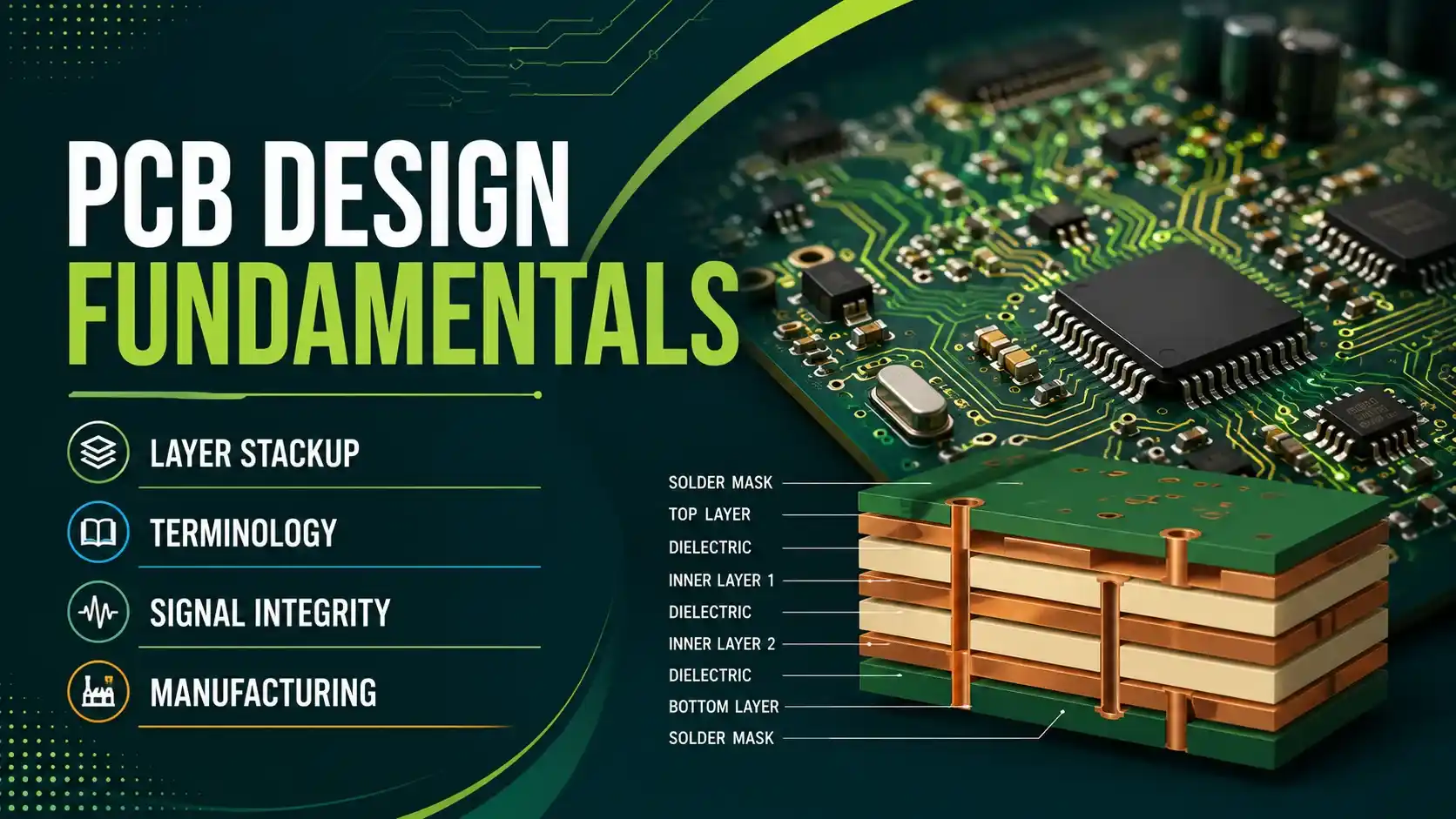
At its core, a PCB is a laminated composite structure composed of alternating layers of conductive metal and insulating dielectric materials. Understanding the four core layers is fundamental to PCB design and analysis.
| Layer | Material | Primary Function | Standard Specs |
|---|---|---|---|
| Silkscreen | Epoxy-based ink | Component labels, logos, warnings | White/Yellow ink, 0.5–1.0 mil thickness |
| Solder Mask | Liquid Photoimageable Polymer | Electrical insulation, protection | Green/Black/Blue, 0.8–1.2 mil thickness |
| Copper Layer | Electrodeposited Foil | Conductive paths, power/ground planes | 0.5 oz (17.5 μm) to 2 oz (70 μm) |
| Substrate (Core) | Glass-reinforced epoxy / Ceramic | Structural base & dielectric insulation | FR-4 (Tg 130–180°C, εr ≈ 4.4) |
Layer 1: Substrate (The Dielectric Base)
The substrate forms the structural foundation of the board. It must be electrically insulating while maintaining mechanical stability across varying temperatures and environmental conditions.
FR-4 (Flame Retardant 4)
The most common substrate material. It consists of woven fiberglass cloth impregnated with an epoxy resin binder. Standard FR-4 features a dielectric constant (εr or Dk) of approximately 4.2 to 4.5 and a glass transition temperature (Tg) ranging from 130°C to 180°C.
High-Frequency / RF Substrates
Standard FR-4 absorbs electromagnetic energy at frequencies above 1 GHz. High-frequency boards use PTFE (Teflon) or hydrocarbon ceramic laminates, such as Rogers materials, with much lower dielectric loss (loss tangent tan δ < 0.002) to preserve signal integrity.
Polyimide
A flexible, high-temperature polymer used as the base for Flexible PCBs (Flex Circuits). It withstands high thermal stress and repeated mechanical bending.
Aluminum / Metal Core (MCPCB)
Used in ultra-high-power LED arrays and power supplies. A metal base, usually aluminum, laminated with a thin, highly thermally conductive dielectric layer helps conduct heat away from components.
Layer 2: Copper Layer (The Conductive Pathways)
Laminated onto the substrate is a thin layer of copper foil. Copper is selected for its high electrical conductivity, ease of soldering, and affordability.
Copper thickness in the electronics industry is specified in ounces per square foot (oz/ft², often shortened to "oz"):
- 0.5 oz Copper (≈17.5 μm / 0.7 mil): Standard for inner signal layers and fine-pitch surface-mount devices (SMD)
- 1.0 oz Copper (≈35 μm / 1.4 mil): The industry standard for outer layers in standard consumer electronics
- 2.0 oz+ Heavy Copper (≥70 μm / 2.8 mil): Required for high-current power distribution, motor drives, and industrial power converters
The electrical resistance (R) of a copper trace depends directly on its physical dimensions and temperature:
- ρ is the electrical resistivity of copper (≈1.68 × 10⁻⁸ Ω·m at 20°C)
- L is the length of the trace
- W is the trace width
- t is the copper thickness
Layer 3: Solder Mask (The Protective Shield)
Solder mask is a liquid photoimageable polymer resin applied over the entire surface of the PCB, leaving only designated copper pads exposed.
Primary Purpose: It prevents molten solder from bridging adjacent copper traces during automated soldering processes, protecting traces from oxidation, dust, and moisture.
Colors: While green is the classic color, offering the highest visual contrast for manual inspection and the lowest historical manufacturing cost, solder mask is routinely applied in red, blue, black, white, and clear variants.
Layer 4: Silkscreen (The Human Interface)
The silkscreen, or legend, is an epoxy-based ink printed on top of the solder mask. It contains essential visual indicators for assembly technicians, repair personnel, and automated optical systems:
- Component reference designators (e.g., R10, C4, U1)
- Pin 1 markers for integrated circuits (ICs) and polarity markings for diodes/capacitors
- Test points, revision numbers, barcodes, and safety warnings
2. Fundamental PCB Terminology and Geometry
To read a datasheet or communicate with a PCB fabricator, you must master the structural language of circuit boards. A typical cross section runs, from top to bottom: solder mask, top copper with an SMT pad, the substrate core with a plated via barrel running through it, bottom copper, and solder mask again, with traces running along the copper layers on either side.
Trace
An etched copper path running along a PCB layer designed to transmit electrical signals or power.
Pad (Land)
An exposed area of copper where a component lead is soldered. Pads are classified into SMT pads (flat surface pads) and Through-Hole pads (plated rings surrounding a drilled hole).
Via
A copper-plated hole drilled through one or more layers of the board to establish electrical connections between different signal or power layers.
Pour / Ground Plane
A continuous sheet of copper covering a large region or entire layer of the PCB. It acts as a low-impedance ground return path, assists in heat dissipation, and minimizes electromagnetic interference (EMI).
Via Types
| Via Type | Description |
|---|---|
| Through-Hole Via | Drilled entirely through the board from top to bottom |
| Blind Via | Connects an outer layer to one or more inner layers without penetrating the entire board |
| Buried Via | Connects internal layers only, completely hidden from the outer top and bottom surfaces |
| Microvia | Ultra-small laser-drilled vias, typically <150 μm in diameter, used in High-Density Interconnect (HDI) boards like modern smartphones |
Plated Through-Hole (PTH): A hole with copper plated on its inner walls, designed to accept axial or radial component leads, such as heavy connectors or large electrolytic capacitors.
Non-Plated Through-Hole (NPTH): Unplated drilled holes used exclusively for mechanical mounting, such as screw holes or alignment pins.
A trace, a pad, and a via are the three building blocks of every PCB layout. Almost every other design rule exists to control how these three elements behave under real electrical and thermal stress.
3. Classifications: Rigid, Flex, and High-Density PCBs
PCBs are tailored to fit distinct mechanical, space, and electrical requirements.
| By Layers | By Flexibility | By Technology |
|---|---|---|
| Single-Sided | Rigid | High-Density Interconnect (HDI) |
| Double-Sided | Flexible (Flex) | High-Frequency / RF |
| Multilayer (4–32+) | Rigid-Flex | Metal-Core (MCPCB) |
Layer-Based Classifications
Single-Sided PCBs: Contain copper tracks on only one side of the substrate. They are inexpensive and used in basic consumer items like remote controls, power supplies, and LED light bulbs.
Double-Sided PCBs: Feature copper tracks on both top and bottom surfaces. Plated through-holes (vias) connect circuits on both sides. This is the entry point for most custom electronics.
Multilayer PCBs: Contain 4, 6, 8, or up to 32+ conductive layers stacked together with alternating pre-impregnated dielectric layers (prepreg). Essential for complex microprocessors, modern graphics cards, and computing hardware.
Structure-Based Classifications
Flex PCBs: Manufactured on thin, flexible polyimide backings. They can bend, twist, and fit into tight non-planar spaces, eliminating bulk wires and heavy connectors.
Rigid-Flex PCBs: Hybrid structures integrating rigid PCB sections connected by flexible polyimide ribbons. Commonly found in aerospace electronics, medical devices, and foldable smartphones.
4. Signal Integrity and Board Physics
As switching speeds and clock frequencies increase, into megahertz and gigahertz ranges, traces can no longer be treated as simple zero-resistance wires. They behave as transmission lines.
A microstrip, the most common high-speed trace geometry, is a trace of width w and thickness t running over a dielectric substrate of height h and dielectric constant εr, referenced to a ground plane below.
Trace Current Carrying Capacity (IPC-2221)
Designers must size traces appropriately to prevent excessive temperature rise caused by I²R resistive heating. According to the industry standard IPC-2221, the maximum current I, in Amperes, for an external trace is governed by:
- k is a derating constant (0.048 for external layers, 0.024 for internal layers due to reduced heat dissipation)
- ΔT is the allowed temperature rise above ambient, in °C
- A is the cross-sectional area of the trace, in mils²
Rule of Thumb: A 1 oz copper trace on an outer layer running at room temperature requires approximately 1 mm (40 mils) of trace width per 1 Ampere of current to keep heating under 10°C.
Characteristic Impedance (Z₀)
For high-speed signals, such as USB 3.0, PCIe, HDMI, and Ethernet, signal traces must be routed with controlled impedance to prevent signal reflections and data degradation.
For a single-ended microstrip, a trace on an outer layer running over an internal reference ground plane, characteristic impedance Z₀ can be approximated as:
- εr is the relative permittivity (dielectric constant) of the substrate
- h is the substrate thickness between the trace and ground plane
- w is the trace width
- t is the copper thickness
To prevent signal degradation, the trace's characteristic impedance must match the source and load impedance, most commonly 50 Ω single-ended or 100 Ω differential.
5. The End-to-End PCB Design and Manufacturing Workflow
Designing and bringing a printed circuit board to market follows a rigid engineering lifecycle.
Schematic Capture
Engineers design the logical circuit diagram using an EDA tool, such as Altium Designer, KiCad, or OrCAD. Every electrical component is represented by a schematic symbol, and connections between pins are defined as logical "Nets."
Component Footprint Mapping
Every symbolic component is paired with a physical 2D footprint (land pattern) following IPC-7351 guidelines. Footprints specify exact pad sizes, spacing, pin numbers, and mechanical outlines needed for soldering.
PCB Board Outline and Constraint Setup
The board perimeter is defined based on mechanical enclosure requirements, often imported via DXF/STEP files. Design rules (DRC) are established for trace widths, minimum clearances, via sizes, and layer stackups.
Floorplanning and Placement
Components are placed on the board surface. Critical high-speed ICs, power supplies, and connectors are placed first, prioritizing short signal loops, low noise, and effective thermal paths.
Trace Routing and Plane Definition
Copper connections (traces) are routed between pads following netlist requirements. Differential pairs are length-matched, high-speed signals are kept over solid reference ground planes, and power distribution networks (PDN) are copper-poured.
Design Rule Check (DRC) and Verification
Automated software checks evaluate the completed board against fabricator capabilities, detecting short circuits, insufficient clearances, dangling traces (stubs), or unrouted nets.
Output File Generation (CAM Export)
The completed design is exported into manufacturing-ready formats: Gerber Files (RS-274X / Gerber X2) as individual vector image files for each layer, an Excellon Drill File specifying coordinates and tool sizes for all drilled holes, and IPC-2581 / ODB++ as modern single-file formats containing full layout, stackup, and netlist intelligence.
Fabrication (Fab) and Assembly (PCBA)
The PCB fabricator etches the raw copper, laminates layers, drills holes, and coats pads. Next, the PCBA house applies solder paste using a laser-cut stencil, places components via automated Pick-and-Place robots, and runs boards through a thermal Reflow Oven.
6. Surface Finishes Comparison
Bare copper oxidizes quickly in air, destroying solderability. To protect exposed pads prior to assembly, fabricators apply a chemical surface finish.
| Surface Finish | Process Description | Key Advantages | Disadvantages / Cost |
|---|---|---|---|
| HASL (Hot Air Solder Leveling) | Board is dipped in molten solder and blown flat with air knives | Inexpensive, long shelf life, robust solder joints | Uneven surface profile; unsuitable for fine-pitch BGAs |
| ENIG (Electroless Nickel Immersion Gold) | Chemical plating of thin gold over nickel layer | Flattest pads, great for fine-pitch BGAs, excellent corrosion resistance | More expensive; potential for "black pad" structural defects |
| OSP (Organic Solderability Preservative) | Water-based organic compound applied selectively to copper | Flat surface, low cost, eco-friendly | Short shelf life; sensitive to repeated handling and thermal cycles |
| Immersion Silver (IAg) | Direct displacement plating of silver onto copper | Extremely flat, highly conductive, excellent for RF signals | Tarnishes when exposed to airborne sulfur; strict handling required |
7. Design for Excellence (DFX) Principles
Designing a board that functions on a schematic is only half the battle. Successful engineers design for Manufacturability (DFM) and Assembly (DFA) to ensure high yields and reliable field operation.
DFM: Design for Manufacturability
- Aspect Ratio: The ratio of board thickness to drilled hole diameter (T/D). Standard drills should keep aspect ratios below 8:1, e.g. a 1.6 mm thick board should have via holes no smaller than 0.2 mm, to ensure electroplating chemicals flow completely through holes.
- Annular Ring Clearance: The width of copper pad remaining around a drilled via hole. If the drill sways slightly, an insufficient annular ring causes "breakout," breaking the electrical circuit.
- Copper Balance: Maintain relatively equal copper coverage on opposing layers. Unbalanced copper layers cause thermal expansion mismatches during reflow, resulting in severe board warping (bow and twist).
DFA: Design for Assembly
- Fiducial Marks: Place at least three L-shaped or circular copper reference points on the outer board corners. Automated vision systems use fiducials to align pick-and-place nozzles with high precision (<10 μm).
- Thermal Relief Pads: When connecting a component pad directly to a broad copper plane, surround the pad with thin copper spokes (a thermal cross) rather than solid copper. Solid copper drains heat during soldering, causing cold solder joints or component "tombstoning," where a surface-mount chip lifts up on one side like a tombstone.
A solid copper pad bleeds heat straight into the surrounding plane. A thermal relief pad, ringed with thin copper spokes, keeps that heat contained right where the solder joint needs it during reflow.
8. Emerging Trends in PCB Technology
As electronics become smaller, faster, and more integrated, PCB manufacturing continues to evolve.
- High-Density Interconnect (HDI): Utilizing microvias, laser drilling, and trace/space widths below 75 μm (3 mils) to fit powerful computer chips into wearable form factors.
- Embedded Components: Active ICs and passive resistors/capacitors are increasingly embedded directly inside internal substrate layers rather than mounted on top surfaces, freeing up surface space and shortening high-speed signal paths.
- Rigid-Flex Miniaturization: Replacing board-to-board ribbon cables with continuous, integrated rigid-flex structures in high-vibration automotive and defense systems.
- Additive Manufacturing / 3D Printed Electronics: Utilizing conductive inks to print multilayer structures on demand, enabling rapid prototyping and non-planar 3D geometry circuits.
Summary Checklist for Hardware Engineers
Before submitting your PCB files for manufacturing, ensure you complete this final checklist:
- Rule Verification: Run a complete Design Rule Check (DRC) with zero remaining errors.
- Manufacturability Check: Verify that minimum trace widths, hole sizes, and clearances meet your fabricator's capabilities.
- Impedance Verification: Confirm that controlled impedance traces match the layer stackup specs from your vendor.
- Mechanical Fit: Verify board dimensions, mounting hole placements, and component heights against your 3D enclosure models.
- Clear Legend: Confirm that all silkscreen text is legible, clear of exposed pads, and properly oriented.
FAQs on PCB Design Fundamentals
You May Also Like
PCB Fundamentals Explained: Types, Features, and Applications
This deeper technical guide builds on the basics. That article covers the nine common PCB board types, six key features, and the seven industries where PCBs show up most, a good starting point before diving into layer stackups and impedance formulas.
Read Full Article →External References
These sources go deeper into the standards referenced throughout this guide.
- IPC-2221, Generic Standard on Printed Board Design, IPC
- Printed Circuit Board, Wikipedia
- Microstrip, Wikipedia
What we learn today
- A PCB stackup is built from four core layers, silkscreen, solder mask, copper, and substrate, each with its own material and function.
- Traces, pads, and vias are the building blocks of every layout, and via type (through-hole, blind, buried, microvia) affects both cost and density.
- Trace current capacity and characteristic impedance are governed by real formulas from IPC-2221 and microstrip theory, not guesswork.
- A rigid engineering workflow, from schematic capture through fabrication and assembly, turns a design file into a physical board.
- DFM and DFA principles, aspect ratio, annular ring clearance, copper balance, fiducials, and thermal relief, are what separate a design that works on paper from one that yields reliably in production.