
A via connects copper traces between layers of a printed circuit board, and choosing the right kind directly shapes cost, density, and signal quality.
Understanding PCB Via Types starts with recognizing that a through hole via passes completely through the board, while a blind or buried via connects only a chosen subset of internal layers.
Via placement decisions build directly on PCB design fundamentals, since layer stackup and routing strategy decide which via style even makes sense for a given board.
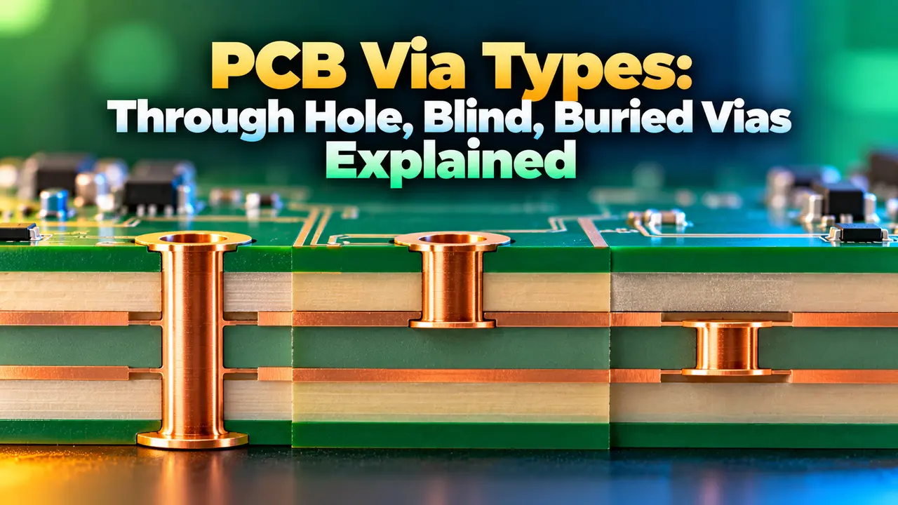
PCB Via Types: The Three Core Categories
A through hole via drills completely from the top layer to the bottom layer, connecting every layer it passes through and remaining the simplest, cheapest option to manufacture.
A blind via starts at an outer layer and stops at an internal layer without reaching the opposite side, freeing up routing space without needing a full drill pass.
A buried via connects two or more internal layers entirely, staying completely hidden inside the board and never appearing on either outer surface at all.
4 Steps in the Via Fabrication Process
Via Types Compared
Passes through all layers, lowest cost, but consumes routing space on every layer.
Connects an outer layer to an inner layer only, saving space on unused layers.
Hidden entirely within internal layers, invisible from either outer surface.
A very small laser drilled via, typically under 150 microns, used in HDI boards.
Cross Section of a Multilayer Board
Via Aspect Ratio Check
Example:
Board thickness = 1.6 mm
Drill diameter = 0.2 mm
Aspect ratio = 1.6 divided by 0.2 = 8 to 1
A high aspect ratio via is harder to plate reliably, which is one reason a well designed ground plane layout often routes around unnecessarily deep via structures.
Where Each Via Type Is Used
Common Mistakes in Via Selection
Specifying blind or buried vias for a design that does not actually need the extra routing density adds unnecessary fabrication cost and lead time without any real benefit.
Ignoring via stub length on high speed signals is another frequent issue, since an unused via barrel segment can act as a small antenna and degrade signal integrity at gigahertz frequencies.
Placing vias too close to fine pitch component pads can cause solder wicking during reflow, pulling solder away from the pad and creating a weak or open joint.
Verifying trace width alongside via placement with a PCB trace width calculator helps catch current density issues at the same time.
Skipping thermal via arrays under power components is a common oversight as well, since a single via rarely conducts enough heat away from a hot running part on its own.
Choosing among the available PCB Via Types without consulting the fabricator's capability list is another practical mistake, since not every shop supports laser drilled microvias or stacked buried structures at a reasonable cost.
Documentation also matters more than many designers expect. Clearly marking which layers each blind or buried via connects on the fabrication drawing prevents costly misunderstandings during the manufacturing quote and build process.
This is similar to how carefully choosing among resistor types needs clear documentation on a bill of materials.
Simulation tools can help validate a via design before committing to fabrication. Modeling the parasitic inductance and capacitance of a via barrel reveals whether it will meaningfully affect signal integrity at the intended operating frequency.
Aspect Ratio Calculator
Reference Document
Watch: Adding Vias in a PCB Stackup
Frequently Asked Questions
Related Articles
- PCB Design Fundamentals
- Ground Plane in PCB Design
- PCB Trace Width Calculator
- Resistor Types Explained
- MOSFET Working Principle
External References
What We Learn Today
- Through hole, blind, and buried vias differ mainly in which layers they connect and how they are manufactured.
- Blind and buried vias save routing space at the cost of higher fabrication complexity and price.
- Aspect ratio, stub length, and thermal relief all deserve attention once a via type has been chosen.