
This circuit copies its input voltage to its output exactly, without amplifying it, and that single trait makes it one of the most quietly useful op amp configurations in analog design.
A Voltage Follower takes advantage of an op amp's near infinite input impedance and near zero output impedance, isolating a sensitive source from a load that would otherwise pull its voltage down.
This circuit is one of the simplest applications built on the general operational amplifier basics every analog design starts from.
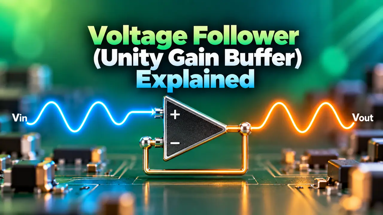
Voltage Follower Working Principle
The op amp's output is fed directly back into its inverting input, forming negative feedback with no resistors in the loop at all.
That direct feedback forces the output voltage to track the non inverting input voltage as closely as the op amp's open loop gain and bandwidth allow.
Because the gain works out to almost exactly one, the circuit passes the input signal through unchanged in amplitude while contributing a large amount of current drive at the output.
4 Steps in Buffered Signal Transfer
Related Buffer Configurations
The classic configuration, offering the highest input impedance and best precision.
A transistor based buffer with lower input impedance but higher current capability.
A FET based buffer offering very high input impedance with moderate drive strength.
Buffer Isolating Source from Load
Closed Loop Gain Check
Example:
Input voltage = 2.5 V
Output voltage = 2.5 V
Gain error mainly comes from open loop gain and offset voltage, not the formula itself
Because there is no resistor network to size, a voltage follower avoids the resistor tolerance and thermal drift issues that affect a standard common emitter amplifier stage.
Where a Voltage Follower Is Used
Common Mistakes When Using a Buffer
Assuming perfect gain accuracy is a common oversight, since real op amps have finite open loop gain and input offset voltage that introduce small but nonzero error.
Ignoring output current limits is another frequent mistake. A buffer with a large input impedance can still be overloaded if the connected load demands more current than the op amp can supply.
This current limit consideration is much like the tradeoffs that matter when selecting resistor types for a power sensitive stage.
Skipping compensation for capacitive loads causes ringing or outright oscillation in some op amps, since a follower configuration has zero phase margin to spare against added output capacitance.
Choosing a general purpose op amp for a high frequency buffering task without checking bandwidth is also common, and it results in signal attenuation well below the intended operating frequency.
Power supply decoupling is often underestimated in buffer stages. A small ceramic capacitor placed close to the op amp's supply pins prevents transient current demands from injecting noise into the signal path.
Input bias current is another subtle source of error, especially with high source impedance. Even a few nanoamps of bias current flowing through a large source resistance can create a measurable offset at the output.
Choosing between a bipolar and a CMOS input op amp changes this tradeoff considerably, since CMOS inputs typically offer far lower bias current at the cost of somewhat higher input offset voltage drift, a tradeoff similar to the ones seen in cascode amplifier design.
Loading Error Calculator
Reference Document
Watch: Op Amp Voltage Follower Explained
Frequently Asked Questions
Related Articles
- Operational Amplifier Basics
- Common Emitter Amplifier
- Cascode Amplifier Working Principle
- Resistor Types Explained
- MOSFET Working Principle
External References
What We Learn Today
- A unity gain buffer copies its input voltage exactly while providing high input impedance and low output impedance.
- Direct feedback with no resistors sets the gain to one, avoiding resistor tolerance and drift issues.
- Stability with capacitive loads and output current limits deserve attention despite the circuit's simplicity.