
A semiconductor is not simply "a material between a conductor and an insulator." The real answer sits in band theory, the energy gap between a material's valence band and conduction band, which doping lets engineers tune by many orders of magnitude on command.
This guide works through the actual band gap numbers, how N type and P type doping really work, and why conductivity rises with temperature, backed by a carrier concentration calculator built on the mass action law.
A semiconductor is a crystalline material, most commonly silicon, whose electrical conductivity sits between that of a conductor and an insulator. Its forbidden energy gap is small enough that heat, light or an applied voltage can promote electrons from the valence band into the conduction band.
That single property, a controllable and comparatively small band gap, is what allows engineers to precisely tune a semiconductor's conductivity through doping.
It is the physical foundation underneath every diode, transistor and integrated circuit in use today.
Ask most people what a semiconductor is and they will say it conducts electricity a little, more than an insulator, less than a conductor. That is true, but it explains nothing about why the material behaves that way or why it is so useful.
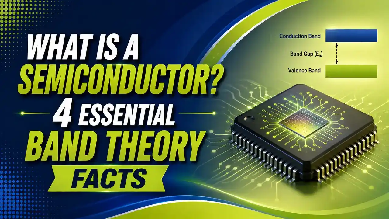
The actual answer involves band theory: every solid has a valence band, where electrons are bound to atoms, and a conduction band, where electrons move freely and carry current. The energy gap between the two decides everything.
In a conductor, the two bands overlap, so electrons are always free to move. In an insulator, the gap is so large that almost no electron can cross it under normal conditions.
A semiconductor sits in between, with a gap small enough to cross under real world conditions like room temperature heat or an applied electric field.
What Actually Makes a Material a Semiconductor
The formal boundary most semiconductor physics references use is a band gap below roughly 3.0 electron volts. Below that threshold, thermal energy at room temperature is enough to excite a meaningful population of electrons across the gap and into the conduction band.
Silicon, the material behind the overwhelming majority of commercial electronics, has a band gap of about 1.12 electron volts at room temperature.
Germanium, an earlier semiconductor material now mostly used in specialty devices, has a narrower gap of about 0.67 electron volts, which is why germanium diodes conduct at a lower forward voltage than silicon diodes.
Compound semiconductors extend the range further in both directions. Gallium arsenide has a band gap near 1.42 electron volts and switches faster than silicon, which is why it shows up in high frequency radio frequency circuits.
Wide band gap materials like silicon carbide and gallium nitride sit above 3 electron volts and tolerate far higher voltage and temperature, which is why they are displacing silicon in power electronics and electric vehicle inverters.
| Material Class | Typical Resistivity | Band Gap | Example |
|---|---|---|---|
| Conductor | Roughly 10 to the negative 8 to 10 to the negative 6 ohm meter | Bands overlap, effectively zero gap | Copper, aluminum, silver |
| Semiconductor | Roughly 10 to the negative 5 to 10 to the 6 ohm meter, tunable by doping | Roughly 0.1 to 3.0 electron volts | Silicon, germanium, gallium arsenide |
| Insulator | Greater than 10 to the 8 ohm meter | Greater than 3.0 electron volts | Glass, rubber, ceramic |
Intrinsic vs Extrinsic Semiconductors
An intrinsic semiconductor is chemically pure, no deliberate impurity added at all. Pure silicon and pure germanium both have four valence electrons, forming a stable diamond cubic crystal lattice where every atom shares its four valence electrons with four neighbors in covalent bonds.
At absolute zero, that lattice has no free carriers at all, every electron is locked into a bond.
At room temperature, thermal energy breaks a small number of those bonds, creating an electron in the conduction band and leaving behind a hole in the valence band.
This is why intrinsic silicon has a small but genuinely useful intrinsic carrier concentration of about 1.5 times 10 to the 10 electrons per cubic centimeter at room temperature.
An extrinsic semiconductor is the same base crystal deliberately doped with a controlled trace of a different element, typically at concentrations between one part per million and one part per hundred million of the host atoms.
That tiny addition changes the carrier population by many orders of magnitude, which is the entire reason doping is useful.
N Type and P Type Semiconductors Explained
Doping silicon with a pentavalent element, one with five valence electrons such as phosphorus, arsenic or antimony, produces an N type semiconductor.
Four of the dopant atom's five valence electrons bond normally with the surrounding silicon lattice, and the fifth is only loosely held, free to join the conduction band with very little thermal energy.
Electrons become the majority carrier and holes the minority carrier in this material.
Doping silicon with a trivalent element instead, one with three valence electrons such as boron, gallium or aluminum, produces a P type semiconductor.
The dopant atom can only complete three of the four covalent bonds the lattice expects, leaving a vacancy, a hole, that a neighboring electron can hop into.
Holes become the majority carrier and electrons the minority carrier in this material.
Neither N type nor P type material is charged overall. Every dopant atom is still electrically neutral in the lattice, it has simply donated a free electron or accepted a bonding electron.
What changes is the population of mobile carriers available to conduct current, not the net charge of the crystal.
Intrinsic Silicon and Germanium
Pure, undoped crystal. Carrier concentration is fixed by temperature alone, around 1.5 times 10 to the 10 per cubic centimeter for silicon at room temperature.
N Type (Donor Doped)
Doped with phosphorus, arsenic or antimony. Free electrons become the majority carrier, holes the minority carrier.
P Type (Acceptor Doped)
Doped with boron, gallium or aluminum. Holes become the majority carrier, electrons the minority carrier.
Compound Semiconductors
Gallium arsenide, silicon carbide and gallium nitride extend band gap, speed and power handling well beyond plain silicon.
Semiconductor Doping and Carrier Concentration Estimator
This calculator applies the mass action law used throughout semiconductor physics, majority carrier concentration times minority carrier concentration equals the intrinsic carrier concentration squared.
Enter a base material, a doping type, and a doping concentration to see the resulting majority and minority carrier populations and the ratio between them.
How Doping Actually Happens During Manufacturing
Real semiconductor manufacturing introduces dopants through one of two controlled processes, thermal diffusion or ion implantation, not by mixing powders together like a metallurgist alloying steel.
Thermal diffusion heats the silicon wafer in the presence of a dopant source gas or solid source, letting dopant atoms migrate into the crystal lattice from the surface inward, similar to how a scent slowly spreads through a still room.
It is simple and inexpensive, but the resulting doping depth and concentration profile are harder to control precisely.
Ion implantation instead accelerates dopant ions to high energy in a particle accelerator and fires them directly into the wafer, where they physically embed themselves at a depth controlled by the acceleration energy.
This is the dominant method in modern integrated circuit fabrication because the dose and depth can be controlled with extreme precision, which matters enormously once transistor features shrink to nanometer scale.
Energy Bands, the Forbidden Gap and Donor and Acceptor Levels
This is the real reason doped silicon conducts so much better than pure silicon at room temperature. An intrinsic crossing needs about 1.12 electron volts.
Ionizing a typical donor or acceptor level, by contrast, needs only a few hundredths of an electron volt, an amount thermal energy at room temperature supplies easily.
Why Semiconductor Conductivity Rises With Temperature
A conductor and a semiconductor respond to heat in opposite directions, and mixing this up is a common source of confusion for anyone new to the topic.
Heating a conductor increases lattice vibration, which scatters the free electrons already present more often and increases resistance. A conductor therefore has a positive temperature coefficient of resistance, resistance rises as it heats up.
Heating a semiconductor does the opposite overall. Yes, lattice scattering increases just like in a conductor, but that effect is completely overwhelmed by a much larger one, more thermal energy generates far more electron hole pairs across the band gap.
Carrier concentration grows exponentially with temperature, so total conductivity rises even though each individual carrier is scattered slightly more often. A semiconductor therefore has a negative temperature coefficient of resistance overall.
This is also why unprotected semiconductor junctions are vulnerable to thermal runaway if they are not managed correctly.
Real World Applications of Semiconductor Materials
A single P type region next to a single N type region forms a PN junction, the foundation of the diode, which only lets current flow in one direction.
Stack two junctions together in the right arrangement and the result is a bipolar junction transistor, capable of amplifying or switching a signal.
Metal oxide semiconductor field effect transistors, the workhorse of modern digital logic, use a controlled electric field rather than direct current injection to turn a conduction channel on and off.
That field effect approach is what allows billions of them to be packed onto a single integrated circuit with manageable power consumption.
Beyond digital logic, semiconductor junctions convert light into electricity in photovoltaic solar cells, convert electricity into light in light emitting diodes and laser diodes, and sense temperature, pressure, and magnetic fields in countless industrial instrumentation devices.
Semiconductor Material Selection Do's and Don'ts
✓ Do
- Match the band gap to the application, wide band gap materials for high voltage and high temperature power circuits
- Remember doping changes carrier concentration, not the overall electrical neutrality of the crystal
- Account for a semiconductor junction's negative temperature coefficient in thermal design
- Treat published intrinsic carrier concentration values as room temperature approximations, they shift meaningfully with temperature
✗ Don't
- Assume every semiconductor behaves like silicon, germanium and gallium arsenide have genuinely different band gaps and switching behavior
- Confuse N type material with a negative net charge, or P type with a positive net charge, both stay neutral overall
- Ignore thermal runaway risk in power semiconductor design, rising temperature increases carrier concentration further
- Treat doping concentration and majority carrier concentration as unrelated numbers, at typical doping levels they are approximately equal
Resources on Semiconductor Physics and Materials
What Is a Semiconductor Questions Engineers Ask
External References
- WatElectronics: Intrinsic Semiconductor and Extrinsic Semiconductor, Energy Band and Doping
- WaferWorld: Band Gap in Semiconductors, All You Need to Know
What We Learn Today
- A semiconductor's defining property is a comparatively small band gap, roughly under 3 electron volts, that separates its valence band from its conduction band.
- Doping with pentavalent or trivalent elements creates N type or P type material by adding a shallow donor or acceptor energy level, not by changing the crystal's overall electrical charge.
- The mass action law ties majority and minority carrier concentration together through the intrinsic carrier concentration, no matter how heavily a material is doped.
- Semiconductor conductivity rises with temperature because carrier generation dominates lattice scattering, the opposite of how a metal conductor behaves.