
The IGBT (Insulated Gate Bipolar Transistor) combines the MOSFET gate with the BJT output stage -- the dominant switching device in power electronics, used in VFDs, inverters, and EV drives. See the semiconductor fundamentals guide for the underlying physics.
This guide covers the structure, working principle, key parameters, comparison with MOSFET and BJT, and the main industrial applications.
Gate emitter voltage above 4 to 8 V turns this device on; removing the gate voltage turns it off. The gate draws almost no steady state current -- voltage controlled like a MOSFET, with output behaving like a BJT.
Why the IGBT Working Principle Combines Two Technologies

Before this device was developed, engineers had to choose between two imperfect options. The power BJT handled high voltage but needed a large base drive current and switched slowly.
The power MOSFET switched fast but had high on state resistance at high voltages.
The IGBT solves this by combining both -- a MOS gate structure controlling an internal bipolar output stage.
The result is MOSFET input simplicity with BJT output performance. The key enabling mechanism is conductivity modulation. Click any term to expand.
IGBT Structure and Terminal Identification
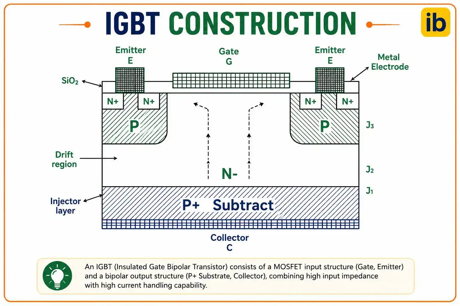
This device has three terminals: Gate (G), Collector (C), and Emitter (E).: Gate (G), Collector (C), and Emitter (E). These correspond roughly to the Gate, Drain, and Source of a MOSFET, or the Base, Collector, and Emitter of a BJT.
Internally: P+ collector, N drift, P body, N+ emitter. Thin oxide insulates the gate from the P body.
When gate voltage is applied, an N type channel forms and electrons flow from emitter to collector, forward-biasing the P+/N junction and triggering bipolar conduction.
Turn on and Turn off Sequence
Turn-on: Apply +15 V to the gate. The MOS channel forms and electrons flow into the N- drift region. The P+ collector injects holes. Conductivity modulation reduces N- resistance. VCE falls to VCE(sat) within microseconds.
Turn-off: Remove gate voltage. The MOS channel collapses and electron flow stops.
Stored minority carriers in the N drift region take a finite time to recombine -- producing the tail current that increases switching loss at high frequency.
IGBT vs MOSFET vs BJT: Full Comparison
| Parameter | Power BJT | Power MOSFET | IGBT |
|---|---|---|---|
| Drive type | Current driven (base current needed) | Voltage driven (gate voltage) | Voltage driven (gate voltage) |
| On state drop | Low VCE(sat) ~0.5 to 1 V | High at high voltage (I² × RDS(on)) | Low VCE(sat) ~1 to 3 V (conductivity modulation) |
| Switching speed | Slow (microseconds) | Very fast (nanoseconds) | Fast (microseconds), limited by tail current |
| Voltage rating | Up to ~1,400 V | Practical up to ~900 V (SiC higher) | 600 V to 6,500 V widely available |
| Current rating | High, but thermally limited | Limited by RDS(on) at high voltage | High -- 25 A to 3,600 A in standard modules |
| Drive circuit complexity | High (base current source needed) | Low (gate voltage only) | Low (gate voltage only, same as MOSFET) |
| Typical frequency | Up to ~5 kHz | Up to 1 MHz (Si), higher with SiC | 1 to 50 kHz typical |
| Main applications | Legacy power supplies | Low voltage high-speed switching, SMPS | VFDs, inverters, traction, EV drives, welding |
Power Loss Calculator
Industrial Applications of the IGBT
Variable Frequency Drives (VFD)
VFDs use a three phase inverter bridge to convert fixed frequency AC to variable frequency AC for motor speed control. Each bridge leg has two IGBTs and two freewheeling diodes.
Switching frequency is typically 2 to 16 kHz. See the MOSFET guide for comparison at lower voltages.
Solar and Wind Inverters
Grid tied renewable energy inverters convert DC from solar panels to grid frequency AC. These devices switch at 10 to 20 kHz with DC bus voltages of 400 to 1,000 V.
The low VCE(sat) keeps conduction losses manageable at continuous high currents.
Electric Vehicle Motor Drives
EV traction inverters operate from 400 V or 800 V battery packs at 200 to 800 A. Modules rated at 650 V to 1,200 V with low VCE(sat) are standard.
Wide-bandgap SiC MOSFETs are beginning to replace them in new EV designs, but IGBTs remain dominant in most current production vehicles.
Industrial Welding Machines
Inverter welding machines switch at 20 to 100 kHz, converting mains power to high frequency AC, passing it through a small transformer, rectifying it, and delivering DC welding current.
The high frequency allows a much smaller transformer. See the arc flash guide for electrical safety and the power factor guide for inverter power quality.
Watch: IGBT Working Principle Explained
IGBT Working Principle Questions
External References
- Insulated Gate Bipolar Transistor (IGBT) -- Electronics Tutorials
- IGBT Working Principle -- GTAKE Power Electronics
What We Learn Today
- The the working principle of this device combines a MOSFET gate (voltage controlled, no base current) with a BJT output stage (low VCE(sat), conductivity modulation)
- Turn-on: apply +15 V gate; MOS channel forms; conductivity modulation reduces N- drift resistance; VCE falls to 1 to 3 V
- Turn-off: remove gate voltage; minority carrier tail current flows until stored carriers recombine -- this limits switching frequency
- IGBT ratings: 600 V to 6,500 V blocking, 25 A to 3,600 A collector current, 1 to 50 kHz switching frequency
- IGBT vs MOSFET: IGBT wins above 400 to 600 V; MOSFET wins below 200 V or above 100 kHz
- Main IGBT applications: VFDs, renewable energy inverters, EV motor drives, and industrial welding machines